Download
1 / 9
100 likes | 218 Views
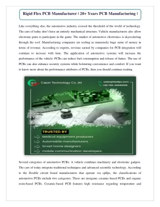
Useful Links<br>http://www.triodepcb.com/<br>http://pageantiques.com.au/<br>http://www.triodepcb.com/index.php/services/electronic-assembly<br>PCB Assembly<br>PCB Manufacturer<br>PCB Manufacturing consists of these steps<br>1)PCB CAM<br> The Gerber or Excellon files in the fabrication data are never used directly on the manufacturing equipment. But always read into the CAM (Computer Aided Manufacturing) software.<br>2)Panelization<br> This is the procedure where the number of PCB's are grouped for manufacturing onto a larger board,this is called by the name panel.<br>3)Copper patterning<br> To replicate the pattern in the fabricator's CAM system on a protective mask on the copper foil PCB layers this is the first step here.Subsequent etching removes the unwanted copper.<br>4)Subtractive,additive and semi-additive processes<br> Here subtractive methods remove copper from an entirely copper coated board to leave only the desired copper pattern.<br>5)Chemical etching<br> It is done with ammonium persulfate or ferric chloride.inner layer automated optical inspection(AOI).Afterwards mistakes can not be corrected,the inner layers are given for the complete machine inspection.<br>6)Lamination<br> We have a trace layers inside the board that is Multi-layer printed circuit boards.<br>7)Drilling<br> Holes through a PCB are drilled with small-diameter drill bits that is made of solid coated tungsten carbide.<br> 8)Plating and coating<br> In this step after PCB's are etched and then rinced with water,the solder mask is applied.And then any exposed copper is coated with the solder, nickel/gold, or some other anti-corrosion coating.<br>9)Solder resist application<br>10)Legend printing<br>11)Bare-board test<br>12)Assembly<br>13)Protection and packaging<br>

E N D
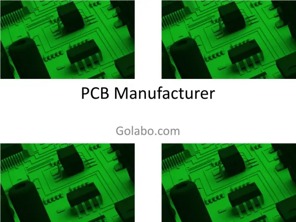
PCB Manufacturer PCB Assembly
PCB Manufacturing consists of these steps 1)PCB CAM 2)Panelization 3)Copper patterning 4)Subtractive,additive and semi-additive processes 5)Chemical etching 6)Lamination
7)Drilling 8)Plating and coating 9)Solder resist application 10)Legend printing 11)Bare-board test 12)Assembly 13)Protection and packaging
PCB Manufacturing steps Are 1)PCB CAM The Gerber or Excellon files in the fabrication data are never used directly on the manufacturing equipment. But always read into the CAM (Computer Aided Manufacturing) software. 2)Panelization This is the procedure where the number of PCB's are grouped for manufacturing onto a larger board,this is called by the name panel.
3)Copper patterning To replicate the pattern in the fabricator's CAM system on a protective mask on the copper foil PCB layers this is the first step here.Subsequent etching removes the unwanted copper. 4)Subtractive,additive and semi-additive processes Here subtractive methods remove copper from an entirely copper coated board to leave only the desired copper pattern.
5)Chemical etching It is done with ammonium persulfate or ferric chloride.inner layer automated optical inspection(AOI).Afterwards mistakes can not be corrected,the inner layers are given for the complete machine inspection. 6)Lamination We have a trace layers inside the board that is Multi-layer printed circuit boards.
7)Drilling Holes through a PCB are drilled with small-diameter drill bits that is made of solid coated tungsten carbide. 8)Plating and coating In this step after PCB's are etched and then rinced with water,the solder mask is applied.And then any exposed copper is coated with the solder, nickel/gold, or some other anti-corrosion coating.
9)Solder resist application 10)Legend printing 11)Bare-board test 12)Assembly 13)Protection and packaging