Download

1 / 17
180 likes | 290 Views
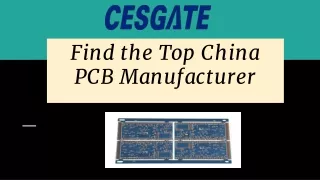
Useful Links<br>http://www.triodepcb.com/<br>http://pageantiques.com.au/<br>http://www.heuristic.com.au<br>The Manufacturing Process<br>1)Double-sided PCBs<br>Photoworks-First of all the plots are made and Photoplots are developed according to the data supplied by the customer.<br>Cam-Bearbeitung-The data records from the various software solutions supported in the PCB-POOL are standardized in the Ext. Gerber Format (RS 274X).<br>Material Preparation-The copper-clad panels along with the drill entry material and a back-up-board are then cut to the size.<br>Drilling and pinning-At this stage the reference and tooling holes are drilled.The PCB-POOL panel is then pinned onto the CNC machine.<br>CNC drilling-With the help of CNC drill machines the through-hole plated and component drills are produced.<br>Through-hole plating-Now an electrographic film (e.g Palladium)is electroplated to the wall of the drill cavity,this allows for galvanization with copper to occur at a later stage.

E N D
Double-sided PCBs • Photoworks First of all the plots are made and Photoplots are developed according to the data supplied by the customer.
Cam-Bearbeitung The data records from the various software solutions supported in the PCB-POOL are standardized in the Ext. Gerber Format (RS 274X). • Material Preparation The copper-clad panels along with the drill entry material and a back-up-board are then cut to the size. • Drilling and pinning At this stage the reference and tooling holes are drilled.The PCB-POOL panel is then pinned onto the CNC machine. • CNC drilling With the help of CNC drill machines the through-hole plated and component drills are produced.
Through-hole plating- Now an electrographic film (e.g Palladium)is electroplated to the wall of the drill cavity,this allows for galvanization with copper to occur at a later stage.
Brushing- Because PCB’s must be completely free of grease and dust,they are subjected to rigourous cleaning(eg:by brushing) before proceeding to the next stage. • Resist laminating- Under extreme temperatures and pressures the entire PCB-POOL panel is laminated with a photosensitive dry resist (Laminar 5038).
Resist exposure- Using the previously generated photoplots the resist is exposed to UV light. • Resist development- Through cyclic construction the exposed panel is developed in a 1% sodium carbonate solution.The PCBs are now ready for plating. • Electroplated Conductor Configuration- The tracks and pads which are developed,free of photo resist are copper plated.
Resist stripping- The photoresist is stripped away with a 2.5% caustic potash solution.This lends itself to the immersion and spray coat processes. • Etching- The next step is the spraying on of a coat of ammonia solution onto the copper film,getting rid of any excess copper,while the galvanisedtin protects the tracks and pads. • Tin stripping- Only then will the tin be removed using a nitic acid based tin-stripper.This lends itself to the dipping or spraying processes. • Soldermaskapplication- The soldermask can be applied as a dry film or a liquid lacquer in a hanging casting implement.After this comes the screen-printing and spraying processes.
Soldermaskexposure- Finally using the previously generated photoplots the soldermask is exposed to light. • Soldermaskdevelopment The development of the exposed PCB is in turn achieved through a cyclic construction in a 1% sodium solution.Hence all soldering points and pads,which are to be tin plated later,are cleared of soldermask. • Silkscreen Using a Direct legend Printer,the silkscreen is immediately printed onto the soldermask.In this process the printhead sprays the screen-print,defined by Gerber data,directly onto the PCB. • Burning-in At a temperature of 150 degree C the soldermask is tempered over a period of approx,60 minutes. • Surface finish • Chemical Nickel-Gold (ENIG) The pads freely developed by the solder paste are coated with Chemical Nickel-Gold together with the surface by means of vertical baths. • The advantages as opposed to HAL are stress-free coating and the flat surface.
Hot Air Levelling (HAL) On the surface coating the pads are tin plated in a hot-air tin-plating system at a temperature of around 270 degree C.
Pinning- To prevent the panel from moving during routing,it is pinned down onto the routing machine bed.
Routing In the final stages,the individual PCB’s are routed from the PCB-POOL panel with the aid of a CNC Routing machine.