Download
1 / 12
120 likes | 125 Views
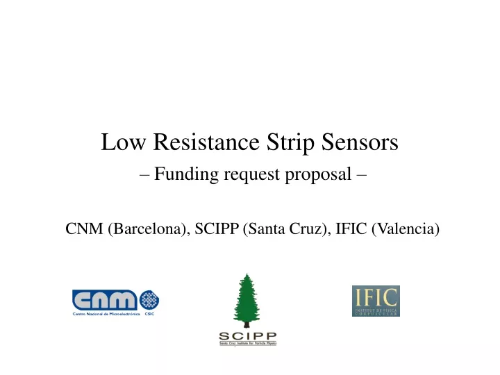
Low Resistance Strip Sensors – Fu nding request proposal –. CNM (Barcelona), SCIPP (Santa Cruz), IFIC (Valencia). The problem. In the scenario of a beam loss, a large charge deposition in the sensor bulk can lead to a local field collapse.

E N D
Low Resistance Strip Sensors– Funding request proposal – CNM (Barcelona), SCIPP (Santa Cruz), IFIC (Valencia)
The problem In the scenario of a beam loss, a large charge deposition in the sensor bulk can lead to a local field collapse. An implant strip potential could reach a significant voltage due to a conducting path to backplane. AC-coupling capacitors can get damaged by the voltage difference between the implant and the readout strip (held to ground by electronics). They are typically qualified to 100 V 2
Micron HPK The current solution • Punch-through (PT) effect is used at Strip end to develop low impedance to the bias line in the case of voltages in excess of the (PT) threshold • Reduce implant distance to bias ring • Placement of the resistor between the implant and bias rail (“transistor effect”). Y. Nobu, et al., NIMA A (2010)doi:10.1016/j.nima.2010.04.080
Punch Through effectiveness Laser tests (SCIPP-Santa Cruz):T. Dubbs et al., IEEE Trans. Nuclear Science 47, pp. 1902 – 1906, 2000. • An IR cutting laser is used to deposit large amounts of charge in the detector bulk • Bias ring held to gnd and Vbias is swept • Implant voltage is measured in DC pad through a pico-probe
Punch Through effectiveness II • “Clamping” of the implant voltage due to PT effect. At a certain value, the implant voltage saturates and do not follow the applied bias. • This is also present after irradiation.
Punch Through effectiveness III Measurements with a large charge injected by a laser pulse showed that the strips can still be damaged The voltages on the opposite end of the strip keep rising well above the 100V objective The large value of the implant resistance effectively isolates the “far” end of the strip from the PT structure leading to the large voltages Near end, plateau for PT structures C. Betancourt, et al. “Updates on Punch-through Protection” ATLAS Upgrade week, Oxford, March 31, 2011. Opposite end, no plateau. 6
Newly proposed solution • To reduce the resistance of the strips on the silicon sensor. • A desired target value is 1.5 kOhm/cm (~ 1 order of magnitude reduction) • Not possible to increase implant doping to significantly lower the resistance. Solid solubility limit of the dopant in silicon + practical technological limits (~ 1 x 1020 cm-3) • Alternative: deposition of Aluminum on top of the implant • A layer of high-quality oxide and nitride with metal strips on top to implement the AC-coupled sensor readout. 7
Technology • Metal layer deposition before the coupling capacitance is defined • MIM capacitors • Low temperature deposited isolation (quality) • PECVD (300-400 ºC) • Use of an Oxide-Nitride-Oxide Layer to avoid pinholes(~200 pF ~1.3 µm ) • Alternatives • Polysilicon + TaSi (tantalum silicide) • Tungsten • Experiments already performed at CNM on smaller dimensions. More experiments to be performed.
Design Python module for creating GDSII stream files (GDS), published under the GNU General Public License (GPL). Requires Python 2.x (Python 2.x is the status quo, Python 3.x is the shiny new thing). Released by Lucas Heitzmann Gabrielli in May 2009, currently in version 0.2.6. Automatic layout generation with GDSPY • Very usefull to automate mask design: • Boolean and slice operations. • Uses NumPy (scientific computing) • We are using currently this to develop the ATLAS-Upgrade endcap prototypes
Timescale • Initial technological experiments (CNM) (Ongoing) • Design definition and mask design and fabrication (CNM, SCIPP) (Started) 1-2 months • Device fabrication at CNM clear room facilities (CNM) 4-5 months • Electrical characterization of the test vehicles (CNM) 1months • Full detector characterization to check for device performance degradation due to new technology, with Alibava System (CNM, IFIC) 2 months • Electrical characterization of the strip resistance and PT structure performance (SCIPP) 1 months • Characterization of sensor protection against beam loss events by implant voltage measurements under a laser pulse (SCIPP) 3 months • Irradiation of devices (neutron/protons) (CNM, SCIPP, IFIC). 4-5 months • Device full characterization after irradiation, with Alibava System (CNM, IFIC) 2 months • Characterization of sensor protection against beam loss events after irradiation (with laser pulse) (SCIPP) 3 months
Funding request The total project costs are 21 k€ (27600 CHF) as detailed: • Wafers : 1000 € (1300 CHF) • 12 FZ HR wafers • Mask Production : 8000€ (10500 CHF) • Fabrication of 12 p-type wafers: 12.000€ (15800 CHF) • The 3 participating institutes ask the RD50 funding for a total of 15000 CHF (3 x 5000 CHF), and will share the extra required budget of 12600 CHF to complete the project. The costs of the required dicing, packaging or wire-bonding plus the initial experiments will also be covered by the institutes.
Summary • Low Resistance Strip Sensors Proposal • CNM-Barcelona, SCIPP-Santa Cruz, IFIC-Valencia • A run of detectors with the following features: • Full p-type strip detectors (ATLAS Upgrade-like) (~8 masks) • PT structures implemented • Metal layer on top of the strip implant • Automatic design (+ test ttructures) • MIM coupling capacitors • Tests to be performed at CERN and UCSC • This could be a very innovative solution for new generations of long-strip detectors and with great applications in future HEP experiments. 12