Download
1 / 16
160 likes | 220 Views
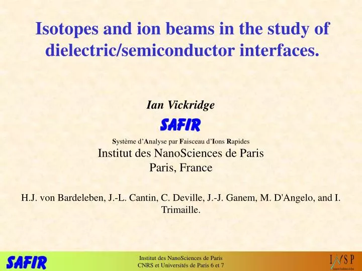
Isotopes and ion beams in the study of dielectric/semiconductor interfaces. Ian Vickridge S ystème d’ A nalyse par F aisceau d’ I ons R apides Institut des NanoSciences de Paris Paris, France. H.J. von Bardeleben, J.-L. Cantin, C. Deville, J.-J. Ganem, M. D'Angelo, and I. Trimaille.

E N D
Isotopes and ion beams in the study of dielectric/semiconductor interfaces. Ian Vickridge Système d’Analyse par Faisceau d’Ions Rapides Institut des NanoSciences de Paris Paris, France H.J. von Bardeleben, J.-L. Cantin, C. Deville, J.-J. Ganem, M. D'Angelo, and I. Trimaille.
Thin film growth processes Thermal growth Deposition First steps treatment under controlled atmosphere heat Structure, composition of the surface 2D mobility, transport Chemical reaction : thermodynamiques, kinetics Diffusion, atomic transport Épitaxy, chemical order Sticking/chemical reaction Interface formation Epitaxy (or not …) Internal surfaces : interfaces of composition, structure Defects, stress, relaxation Growth => atomic transport Isotopes - 6/7Li, H/D, 3/4He, 10/11B, 12/13C, 14/15N, 16/17/18O, 25/26Mg, 28/29/30Si Growth => défauts electron paramagnetic resonance
+ + n n Thermal oxidation of Si and SiC 16/17/18O2 MOSFET Very high e material Capacitor Electrodes SiO2 29Si, Si13C Diffusion barrier Gate electrode Plug - - - - - + + + + + s gate dielectric SiO2/Si - - - - - • High technological interest • Système modèle • Système très très étudié V e d + + + + + s
Manipulation of the interface Si(nano)/SiO2 (with B. Gallas, C. Kao, and I. Stenger, INSP) pump transfer ? Emission 1.54 mm telecoms … First experiments underway SiO2/Si Interface 15NH3, 15N18O 13C18O, 17/18O2 etc amorphous silica doped Er3+ Study the effects of interface modification on nano-cristaux->Er3+ energy transfer Formation of nanocristals of SiC, or Si with SiC (13C …) 'skin' Modification grain size by selective oxidation and oxynitridation Isotopes, Accel, EPR (large internal surface), TEM, ellipsometry, photoluminescence etc…
Tracing with 29Si, Manipulation of the SiC/SiO2 interface SiC 29Si deposited or implanted (CSNSM, Orsay) SiO2 SiC Ar, NO, CO, NH3, … oxidation then, 18O2 as probe of chemical reactivity of interface SiO2 SiC Initial experiments recently performed : results most promising
With G. Battisitig, A Pongracz, Z. Hajnal MFA-KFKI, Budapest SiC nano-crystals SiO2 Si CO 1100°C SEM image after chemical removal of SiO2 overlayer SiC nano-crystals epitaxially embedded in Si 29Si substrate, Si16O2,Si18O2, 12C16O, 13C18O …
SiC nanocrystals SiO2/Si thermal • (100) Growth mechanisms? Atomic transport mechanisms? Kinetics, activation energies? • (110) • (111)
13C Analysis (work in progress!) Strong narrow (~ 100eV) resonance at 1.746 MeV Nucl Data Tables Ajzenberg-Selove, applies inVickridge thesis 13C(p,g)13C 13C(p,p)13C Strong resonance (50-100 sR) at backward angles near 1.5 MeV Milne PhysRev 1954 in Jarjis, numerous pre-1956 data in Jarmie and Seagrove Strong resonance around 2.7 MeV at backward angle Barnes PhysRev 1965 and Kerr PhysRev 1968 in IBANDL 13C(a,a)13C
13C Analysis 13C(d,p)13C Qm=5952 keV Useful yield in sub 2 MeV range. Marion PhysRev 1956 and Colaux et al NIMB and IBANDL
13C Analysis 13C(d,a)11B Q0= 5167.89 keV Q1= 3043.2 Q2= 722.9 Useful yield in sub 2 MeV range. Marion PhysRev 1956 and Colaux et al NIMB and IBANDL
13C Analysis - Summary 13C(p,g)13C No further work required from ND perspective ? 13C(p,p)13C Useful looking resonance at 1.5 MeV. New measurements needed? s(q)? Evaluation? 13C(a,a)13C Useful looking resonance near 2.7 MeV. New measurements needed? s(q)? Evaluation? 13C(d,p)14C Useful s below 2 MeV. Further measurements needed for succesful valuation? 13C(d,a)11B Useful s below 2 MeV. Some discrepancies. Further measurements needed for succesful valuation?
15N Analysis (work in progress too!) 15N(p,ag)12C Wonderful narrow (G=100eV) resonance at 429 keV widely used by several groups useful? resonance near rising to near 3.5 sR near 900 keV Hagendorn PhysRev 1957 in Jarjis 15N(p,p)15N 15N(a,a)15N Useful? resonance near1900 keV Smotrich PhysRev 1961 from IBANDL
15N Analysis 15N(p,a0)12C Q0= 4965 keV Useful cross section. Widely used. Sawicki NIMB in IBANDL 15N(d,p)16N Q0= 264.53 keV Unusable
15N Analysis 15N(d,a0)13C Q0= 7687 keV Useful s below 2 MeV Sawicki, Vickridge NIMB in IBANDL
15N Analysis - Summary 15N(p,ag)12C No further work required from ND perspective? Useful looking resonance near 900 keV. New measurements needed? s(q)? Evaluation? 15N(p,p)15N Possibly useful resonance near 1900 keV. New measurements needed? s(q)? Evaluation? 15N(a,a)15N 15N(d,a0)13C Useful s below 2 MeV for profiling thicker samples. Some discrepancies, further measurements needed for succesful valuation?
Facilities available at INSP Special UHV and high vacuum furnaces for using (expensive) isotopically labelled gases 2.5 MV Van de Graaff High energy p, d, 3He, a detection cp, g, x channelling Clean room