Download
1 / 19
240 likes | 1k Views
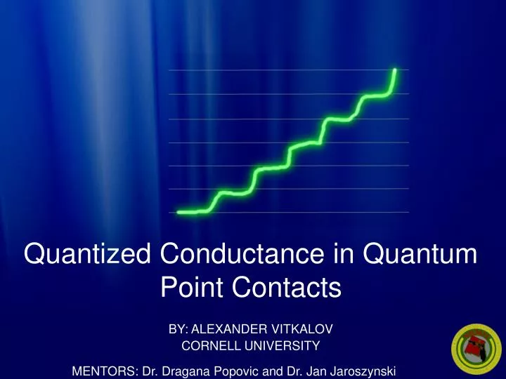
Quantized Conductance in Quantum Point Contacts. BY: ALEXANDER VITKALOV CORNELL UNIVERSITY. MENTORS: Dr. Dragana Popovic and Dr. Jan Jaroszynski. Significance.

E N D
Quantized Conductance in Quantum Point Contacts BY: ALEXANDER VITKALOV CORNELL UNIVERSITY MENTORS: Dr. Dragana Popovic and Dr. Jan Jaroszynski
Significance Since the invention of the first transistor in 1948, electronic devices kept decreasing in size to improve performance and power consumption. At some point, devices would become so small, that they will no longer be governed by diffusive conduction model used today. Quantized Conductance has received much attention recently because of the growing interest in nanoscale electronics and quantum nature of matter. Conductance in nanowires and point contacts needs to be investigated further to create reliable circuitry.
Objective Quantized Conductance > Does it occur at room temperature? > How is it affected by current and voltage? > How does it depend on the type of material?
General Information NATURAL UNITS OF CONDUCTANCE Natural Unit of Conductance is about 1/25812 Ω-1. Which is e2/h. First discovered by Klaus von Klitzing, as a part of his Nobel Prize winning experiment about Quantized Hall Effect. Quantized Conductance in Quantum Point contacts was discovered in 1988 by a group in Cambridge University and University of Delft. WHAT IS CONDUCTANCE? Conductance is an expression of ease with which electric current flows through a substance. 1 Conductance is a reciprocal of resistance and therefore is measured in Ω-1 or S (siemens) ABOUT THE STEPS The steps on the staircase function correspond to integer multiples of quantum unit of conductance 2e2/h, which results from electron spin degeneracy.
General Information What is 2e2/h? 2 1 I=veN/L Current is velocity x charge x number of electrons divided by the length 2 G=I/V=veN/LV Conductance is current divided by voltage 3 ΔE=eV Drop in potential for an electron is charge times the potential 4 G=ve2N/LΔE Substitution of 3 into 2 5 λn=L/n De Broglie wavelength will only have discrete values. (Elementary quantum mechanics for a particle in a box) 6 v=h/Lλ Velocity is h (Planck’s constant) over length times the wavelength 7 vn= nh/Lm Thus the velocity will have discrete values 8 N=2LmΔv/h Number of electrons that contribute to conduction is twice the number of quantum states. Thus N needs to be doubled. 9 K=mv2/2 Kinetic energy of an electron with mass m and velocity v 10 Δ K=mv Δ v/2 Change in Kinetic energy for an electron 11 N = 2L Δ E/vh Combination of 8 and 10 12 G= 2e2/h Combination of 4 and 11 What are Quantum Point Contacts? QPC occur when two wires are in very loose contact. The string of atoms are created between the two contacts. This connection is comparable to the wavelength of the electron.
Experimental Setup Ω (IN PARALLEL) Ω THE CIRCUIT • 0-10V Adjustable voltage source • 10k-100 ohm divider • HP34401A Multimeter • ITHACO 1211 Current Preamplifier to measure the current
Experimental Setup Ω (IN PARALLEL) Ω HP35665A DYNAMIC SIGNAL ANALYZER • Takes a single measurement in less than 4ns. • Measures voltage magnitude of the signal very precisely. • Communicates with a computer through GPIB interface. • Can be controlled by the computer through IEEE 488 protocol.
Experimental Setup Ω (IN PARALLEL) Ω COMPUTER HARDWARE • Dell Dimension PC with Intel Pentium 4(2.8Ghz). • GPIB Board to communicate with instruments. • Fast processor to handle incoming data.
Experimental Setup COMPUTER SOFTWARE • LABVIEW 6.1. • QCE - controls HP35665A DSA. • QCE - processes data, derives conductance from current, records results, graphs data. • EZPLOT – creates histograms of data.
Experimental Setup THE SAMPLE • 0.05mm Gold, .1mm Steel and 0.025mm Aluminum wires were used in this experiment. • Each wire is 3cm in length. • Voltages 0-100mV were applied to the sample. • Sample was gently vibrated so the wires would come in and out of contact with each other.
Results R= V/I * // Voltage approximately constant when the wires are in loose contact*. Rt=[R-(RRES+RV)] // Take in account other factors, so the steps appear at proper values Rn=R/[2e2/h]=R/12906 // Express Resistance in natural units. Gn=1/Rn // Determine conductance by inversing resistance. CALCULATIONS
Results Quantized Conductance Steps (0.05mm Gold Wires at 20mV, RRES=450Ω)
Results Histogram of Quantized Conductance Steps (0.050mm Gold wires at 20mv, RRES=450Ω)
Results Quantized Conductance Steps (0.025mm Aluminum wires at 20mv, RRES=450Ω)
Results Quantized Conductance Steps (0.1mm Steel wires at 10mv, RRES=100Ω)
The bottom line Overall data (1,000,000 points) vs. Selected data (250 points), Gold Wires
The bottom line Our experiment showed that conductance steps can be seen at room temperature, although they are rare. Conductance steps mostly occur when the current is decreasing and is near 0. Conductance steps were seen near 0, while the current was increasing, but they were not as clear. Conductance steps will become less visible as the current through the sample is increased. This can be attributed to electron heating effects2. Gold is the best material to observe quantized conductance. Steel is also good, however, steps aren’t as easily observed at low conductance. Aluminum is by far the worst, due to the problematic point contacts, attributed to oxidation.
References 1 SearchNetworking.com, “SearchNetworking.com Definitions,” Dec 30, 2000. 2 E.L. Foley, D. Candela, K.M. Martini, and M.T. Tuominen. “An Undergraduate laboratory experiment on quantized conductance in nanocontacts,” American Journal of Physics 67, 389(1999).
This presentation was made possible by Florida State University National High Magnetic Field Laboratory Center for Integrated Research and Learning Special thanks to: Dr. Dragana Popovic Dr. Jan Jaroszynski Mr. Jack Challis Dr. Pat Dixon Ms. Gina Hickey CIRL Staff