Download
1 / 70
720 likes | 842 Views
Chapter 6 MOSFET. The MOSFET (MOS Field-Effect Transistor) is the building block of Gb memory chips, GHz microprocessors, analog, and RF circuits. Match the following MOSFET characteristics with their applications: small size high speed low power high gain.

E N D
Chapter 6 MOSFET • The MOSFET (MOS Field-Effect Transistor) is the building block of Gb memory chips, GHz microprocessors, analog, and RF circuits. • Match the following MOSFET characteristics with their applications: • small size • high speed • low power • high gain Modern Semiconductor Devices for Integrated Circuits (C. Hu)
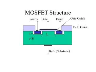
6.1 Introduction to the MOSFET Basic MOSFET structure and IV characteristics + + Modern Semiconductor Devices for Integrated Circuits (C. Hu)
6.1 Introduction to the MOSFET Two ways of representing a MOSFET: Modern Semiconductor Devices for Integrated Circuits (C. Hu)
Early Patents on the Field-Effect Transistor Modern Semiconductor Devices for Integrated Circuits (C. Hu)
Early Patents on the Field-Effect Transistor In 1935, a British patent was issued to Oskar Heil. A working MOSFET was not demonstrated until 1955. Using today’s terminology, what are 1, 2, and 6? Modern Semiconductor Devices for Integrated Circuits (C. Hu)
6.2 MOSFETs Technology Polysilicon gate and 1.2nm SiO2 • 1.2 nm SiO2 used in production. Leakage current through the oxide limits further thickness reduction. Modern Semiconductor Devices for Integrated Circuits (C. Hu)
6.2 Complementary MOSFETs Technology NFET PFET When Vg = Vdd , the NFET is on and the PFET is off. When Vg = 0, the PFET is on and the NFET is off. Modern Semiconductor Devices for Integrated Circuits (C. Hu)
CMOS (Complementary MOS) Inverter A CMOS inverter is made of a PFET pull-up device and a NFET pull-down device. Vout = ? if Vin = 0 V. Modern Semiconductor Devices for Integrated Circuits (C. Hu)
CMOS (Complementary MOS) Inverter • NFET and PFET can be fabricated on the same chip. • basic layout of a CMOS inverter Modern Semiconductor Devices for Integrated Circuits (C. Hu)
6.3 Surface Mobilities and High-Mobility FETs 6.3.1 Surface Mobilities Vg = Vdd , Vgs = Vdd Vds> 0 Ids How to measure the surface mobility: = = m = m × × I W Q v WQ WQ V / L E ds inv inv ns inv ns ds = - m WC ( V V ) V / L gs oxe t ns ds Modern Semiconductor Devices for Integrated Circuits (C. Hu)
C C 1 = - - f oxe E ( V V ) + = + - - f oxe ( E ) ( V V 2 V 2 ) E b t fb st e b t gs t fb st e 2 2 s s = - + e ( Q Q ) / E C » + + t dep inv s oxe ( V V 0 . 2 V ) gs t e 2 C s = - e = + - oxe E Q / E ( V V ) + + b inv s b gs t e V V 0 . 2 V gs t = s 6 T C = - - f oxe oxe ( V V ) gs fb st e s Mobility is a function of the average of the fields at the bottom and the top of the inversion charge layer, Eb and Et . From Gauss’s Law, Eb = – Qdep/es Therefore, Modern Semiconductor Devices for Integrated Circuits (C. Hu)
Surface mobility (cm2/V-s) Universal Surface Mobilities • Surface roughness • scattering is stronger (mobility is lower) at higher Vg, higher Vt, and thinner Toxe. Modern Semiconductor Devices for Integrated Circuits (C. Hu)
EXAMPLE: What is the surface mobility at Vgs=1 V in an N-channel MOSFET with Vt=0.3 V and Toxe=2 nm? Solution: 1 MV is a megavolt (106 V). From the mobility figure, ns=190 cm2/Vs, which is several times smaller than the bulk mobility. Modern Semiconductor Devices for Integrated Circuits (C. Hu)
6.3.2 GaAs MESFET gate source drain metal N-channel + + N N GaAs Semi-insulating substrate MESFET IV characteristics are similar to MOSFET’s but does not require a gate oxide. Question: What is the advantage of GaAs FET over Si FET? Terms: depletion-mode transistor, enhancement-mode transistor Modern Semiconductor Devices for Integrated Circuits (C. Hu) Slide 6-14
6.3.3 HEMT, High Electron Mobility Transistor N-GaAlAs metal gate source drain …....... + + N N Undoped GaAs • A large-Eg semiconductor serves as the “gate dielectric”. • The layer of electrons is called 2D-electron-gas, the equivalent of the inversion or accumulation layer of a MOSFET. Modern Semiconductor Devices for Integrated Circuits (C. Hu) Slide 6-15
6.3.4 JFET gate P+ source drain + + N N-channel N P-Si • The gate is a P+N junction. • The FET is a junction field-effect transistor (JFET). Modern Semiconductor Devices for Integrated Circuits (C. Hu) Slide 6-16
6.4 Vt and Body Effect How to Measure the Vt of a MOSFET A B • Method A. Vt is measured by extrapolating the Ids versus Vgs curve to Ids = 0. • Method B. The Vg at which Ids =0.1mA W/L Modern Semiconductor Devices for Integrated Circuits (C. Hu)
Coxe Cdep MOSFET Vt and the Body Effect • Two capacitors => two charge components • Redefine Vtas Modern Semiconductor Devices for Integrated Circuits (C. Hu)
Body effect: Vtis a function of Vsb. When the source-body junction is reverse-biased, Vt increases. • Body effect coefficient: • a = Cdep/Coxe • = 3Toxe / Wdep MOSFET Vt and the Body Effect Body effect slows down circuits? How can it be reduced? Modern Semiconductor Devices for Integrated Circuits (C. Hu)
Retrograde Body Doping Profiles Wdmax for retrograde doping Wdmax for uniform doping • Wdepdoes not vary with Vsb . • Retrograde doping is popular because it reduces off-state • leakage and allows higher surface mobility. Modern Semiconductor Devices for Integrated Circuits (C. Hu)
Uniform Body Doping When the source/body junction is reverse-biased, there are two quasi-Fermi levels (Efn and Efp) which are separated by qVsb. An NMOSFET reaches threshold of inversion when Ec is close to Efn, not Efp. This requires the band-bending to be 2fB + Vsb, not 2fB. g is the body-effect parameter. Modern Semiconductor Devices for Integrated Circuits (C. Hu)
6.5 Qinv in MOSFET • Channel voltage • Vc=Vsat x = 0 and • Vc=Vdat x = L. • Qinv = – Coxe(Vgs – Vcs – Vt0 –a (Vsb+Vcs) • = – Coxe(Vgs – Vcs – (Vt0 +a Vsb) –a Vcs) • = – Coxe(Vgs– mVcs– Vt) • m º 1 +a =1 + 3Toxe/Wdmax • m is called thebody-effect factororbulk-charge factor Modern Semiconductor Devices for Integrated Circuits (C. Hu)
6.6 Basic MOSFET IV Model Ids= WQinvv= WQinvmnsE = WCoxe(Vgs– mVcs –Vt)mnsdVcs/dx IdsL = WCoxemns(Vgs – Vt – mVds/2)Vds Modern Semiconductor Devices for Integrated Circuits (C. Hu)
Vdsat : Drain Saturation Voltage Modern Semiconductor Devices for Integrated Circuits (C. Hu)
Modern Semiconductor Devices for Integrated Circuits (C. Hu)
Saturation Current and Transconductance • linear region, saturation region • transconductance: gm= dIds/dVgs Modern Semiconductor Devices for Integrated Circuits (C. Hu)
6.7.1 CMOS Inverter--voltage transfer curve Modern Semiconductor Devices for Integrated Circuits (C. Hu)
V ........... dd V V V 1 2 3 ............ C C V 2 V dd V 2 t 3 d V 1 0 t 6.7.2 Inverter Speed – propagation delay Modern Semiconductor Devices for Integrated Circuits (C. Hu)
Vdd Vin Vout 6.7.2 Inverter Speed - Impact of Ion How can the speed of an inverter circuit be improved? Modern Semiconductor Devices for Integrated Circuits (C. Hu)
V dd AB A B Logic Gates This two-input NAND gate and many other logic gates are extensions of the inverter. Modern Semiconductor Devices for Integrated Circuits (C. Hu)
Vdd Vin Vout 6.7.3 Power Consumption Total power consumption Modern Semiconductor Devices for Integrated Circuits (C. Hu)
m E = ns v E + 1 E sat E<<Esat: v = mE ns E>>Esat: v = m Esat ns 6.8 Velocity Saturation • Velocity saturation has • large and deleterious • effect on the Ion of • MOSFETS Modern Semiconductor Devices for Integrated Circuits (C. Hu)
= I WQ v ds inv m dV / dx = - - ns cs I WC ( V mV V ) ds oxe gs cs t dV + 1 cs / E sat dx L V ò ò = m - - - ds I dx [ WC ( V mV V ) I / ] dV E ds oxe ns gs cs t ds sat cs 0 0 m = m - - - I L WC ( V V V ) V I V / E sat ds oxe ns gs t ds ds ds ds 2 6.9 MOSFET IV Model with Velocity Saturation Modern Semiconductor Devices for Integrated Circuits (C. Hu)
W m m - - C ( V V V ) V oxe ns gs t ds ds L 2 = I ds V + 1 ds L E sat long - channel I ds = I ds + 1 V / L E sat ds 6.9 MOSFET IV Model with Velocity Saturation Modern Semiconductor Devices for Integrated Circuits (C. Hu)
dI = ds Solving 0 , dV ds - 2 ( V V ) / m gs t = V dsat + + - 1 1 2 ( V V ) / mE L sat gs t 1 m 1 = + - V V V L E sat dsat gs t 6.9 MOSFET IV Model with Velocity Saturation A simpler and more accurate Vdsatis: 2 v º sat E sat m ns Modern Semiconductor Devices for Integrated Circuits (C. Hu)
- 1 æ ö m 1 ç | = + V ç | dsat - V V L E è ø sat gs t EXAMPLE: Drain Saturation Voltage Question: At Vgs = 1.8 V, what is the Vdsat of an NFET with Toxe = 3 nm, Vt = 0.25 V, and Wdmax = 45 nm for (a) L =10 mm, (b) L = 1 um, (c) L = 0.1 mm, and (d) L = 0.05 mm? Solution:From Vgs , Vt , and Toxe , mns is 200 cm2V-1s-1. Esat= 2vsat/m ns = 8 104V/cm m = 1 +3Toxe/Wdmax = 1.2 Modern Semiconductor Devices for Integrated Circuits (C. Hu)
- 1 æ ö m 1 | ç = + V | ç dsat - V V L E è ø sat gs t EXAMPLE: Drain Saturation Voltage (a) L = 10 mm, Vdsat= (1/1.3V + 1/80V)-1 = 1.3 V (b) L = 1 mm, Vdsat= (1/1.3V + 1/8V)-1 = 1.1 V (c) L = 0.1 mm, Vdsat= (1/1.3V + 1/.8V)-1 = 0.5 V (d) L = 0.05 mm, Vdsat= (1/1.3V + 1/.4V)-1 = 0.3 V Modern Semiconductor Devices for Integrated Circuits (C. Hu)
- 2 long - channel I ( V V ) W dsat gs t = m = I C - - dsat oxe s V V V V 2 mL gs t gs t + + 1 1 L L mE mE sat sat << - L V V E sat gs t = - - I Wv C ( V V L ) mE = - I Wv C ( V V ) dsat sat sat oxe gs t dsat sat oxe gs t Idsat with Velocity Saturation Substituting Vdsatfor Vdsin Idsequation gives: Very short channel case: • Idsatis proportional to Vgs–Vtrather than(Vgs – Vt)2 , not • as sensitive to L as 1/L. Modern Semiconductor Devices for Integrated Circuits (C. Hu)
Measured MOSFET IV What is the main difference between the Vg dependence of the long- and short-channel length IV curves? Modern Semiconductor Devices for Integrated Circuits (C. Hu)
PMOS and NMOS IV Characteristics The PMOS IV is qualitatively similar to the NMOS IV, but the current is about half as large. How can we design a CMOS inverter so that its voltage transfer curve is symmetric? Modern Semiconductor Devices for Integrated Circuits (C. Hu)
6.9.1 Velocity Saturation vs. Pinch-Off Current saturation : the carrier velocity reaches Vsat at the drain. Instead of the pinch-off region, there is a velocity saturation region next to the drain where Qinv is a constant (Idsat/Wvsat). Modern Semiconductor Devices for Integrated Circuits (C. Hu) Slide 6-41
If Idsat0 Vg – Vt , 6.10 Parasitic Source-Drain Resistance • Idsatcan be reduced by about 15% in a 0.1mm MOSFET. Effect is greater in shorter MOSFETs. • Vdsat = Vdsat0 + Idsat (Rs + Rd) Modern Semiconductor Devices for Integrated Circuits (C. Hu)
SALICIDE (Self-Aligned Silicide) Source/Drain contact metal dielectric spacer gate oxide channel N + source or drain NiSi or TiSi 2 2 After the spacer is formed, a Ti or Mo film is deposited. Annealing causes the silicide to be formed over the source, drain, and gate. Unreacted metal (over the spacer) is removed by wet etching. • Question: • What is the purpose of siliciding the source/drain/gate? • What is self-aligned to what? Modern Semiconductor Devices for Integrated Circuits (C. Hu) Slide 4-43
Definitions of Channel Length Modern Semiconductor Devices for Integrated Circuits (C. Hu)
6.11 Extraction of the Series Resistance and the Effective Channel Length Include series resistance, RdsRd + Rs , Modern Semiconductor Devices for Integrated Circuits (C. Hu)
6.12 Velocity Overshoot • Velocity saturationshould not occur in very short MOSFETs. • This velocity overshoot could lift the limit on Ids . • But… Modern Semiconductor Devices for Integrated Circuits (C. Hu)
6.12 Source Velocity Limit = - I Wv C ( V V ) dsat sat oxe gs t • Carrier velocity is limited • by the thermal velocity • with which they enter the • channel from the source. • Idsat = WBvthxQinv • = WBvthxCoxe(Vgs – Vt) • Similar to Modern Semiconductor Devices for Integrated Circuits (C. Hu) Slide 6-47
6.13 Output Conductance • Idsat does NOT saturate in the saturation region, especially in short channel devices! • The slope of the Ids-Vds curve in the saturation region is called the output conductance (gds), • A smaller gds is desirable for a large voltage gain, which is beneficial to analog and digital circuit applications. Modern Semiconductor Devices for Integrated Circuits (C. Hu) Slide 6-48
Example of an Amplifier Vdd R nout nin NFET • The transistor operates in the saturation region. A small signal input, vin, is applied. • The voltage gain is gmsat/(gds + 1/R). • A smaller gds is desirable for large voltage gain. • Maximum available gain (or intrinsic voltage gain) is gmsat/gds Modern Semiconductor Devices for Integrated Circuits (C. Hu) Slide 6-49
6.14 High-Frequency Performance High-frequency performance is limited by input R and/or C. Cutoff frequency (fT) : Frequency at which the output current becomes equal to the input current. Maximum oscillation frequency (fmax) : Frequency at which the power gain drops to unity Intrinsic input resistance Gate-electrode resistance Modern Semiconductor Devices for Integrated Circuits (C. Hu) Slide 6-50