Download
1 / 40
400 likes | 464 Views
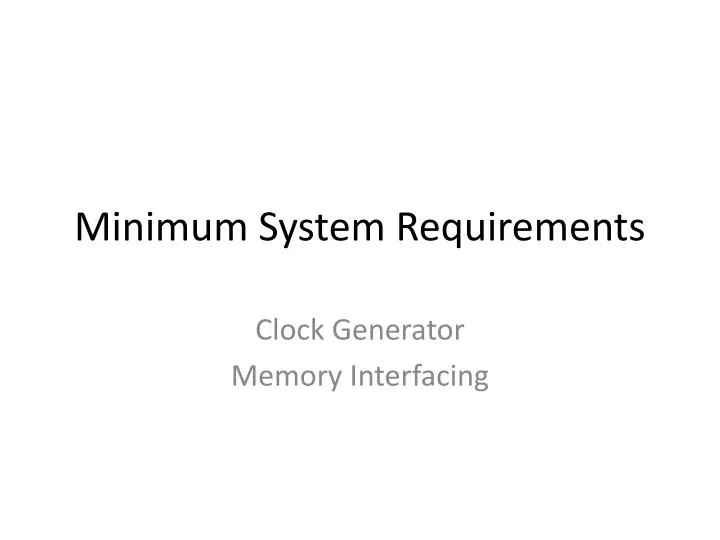
Minimum System Requirements. Clock Generator Memory Interfacing. Timing. CPU. Memory. System bus (data, address & control signals). Serial I/O. Parallel I/O. Interrupt circuitry. System Block Diagram. Crystal oscillator Timing circuitry (counters dividing to lower frequencies).

E N D
Minimum System Requirements Clock Generator Memory Interfacing
Timing CPU Memory System bus (data, address & control signals) Serial I/O Parallel I/O Interrupt circuitry System Block Diagram • Crystal oscillator • Timing circuitry • (counters dividing to lower frequencies) P + associated logic circuitry: • Bus controller • Bus drivers • Coprocessor • ROM (Read Only Memory) (start-up program) • RAM (Random Access Memory) • DRAM (Dynamic RAM) - high capacity, refresh needed • SRAM (Static RAM) - low power, fast, easy to interface Simple (only two wires + ground) but slow. Many wires, fast. At external unexpected events, P has to interrupt the main program execution, service the interrupt request (obviously a short subroutine) and retake the main program from the point where it was interrupt. • Printer (high resolution) • External memory • Floppy Disk • Hard Disk • Compact Disk • Other high speed devices • Printer (low resolution) • Modem • Operator’s console • Mainframe • Personal computer
BHE/S7 BHE/S7 MN/MX MN/MX RD RD WR LOCK M/IO DT/R DEN INTA TEST TEST Required Circuits in Minimum-mode and Maximum-mode Basic Requirements: Power Clock Reset Circuit Memory ( ROM – RAM) GND 1 40 VCC AD14 2 39 AD15 GND 1 40 VCC AD13 3 38 A16/S3 AD14 2 39 AD15 AD12 4 37 A17/S4 AD13 3 38 A16/S3 AD11 5 36 A18/S5 AD12 4 37 A17/S4 AD10 6 35 A19/S6 AD11 5 36 A18/S5 AD9 7 34 AD10 6 35 A19/S6 GND Vcc AD8 8 8086 33 AD9 7 34 AD7 9 32 AD8 8 8086 33 AD6 10 31 RQ/GT0 AD7 9 32 AD5 11 30 RQ/GT1 AD6 10 31 HOLD AD4 12 29 AD5 11 30 HLDA AD3 13 28 S2 AD4 12 29 AD2 14 27 S1 AD3 13 28 AD1 15 26 S0 AD2 14 27 AD0 16 25 QS0 AD1 15 26 NMI 17 24 QS1 AD0 16 25 ALE INTR 18 23 NMI 17 24 CLK 19 22 READY INTR 18 23 GND 20 21 RESET CLK 19 22 READY GND 20 21 RESET Min Mode Max Mode
8284 Clock Generator for 8086 an 18-pin chip • specially designed to be used with 8088/86 microprocessors, • It provides the clock and synchronization for the microprocessor, • also provides the READY signal for the insertion of wait states into the CPU bus cycle.
Memory Interfacing Timing Memories
Read Cycle Min mode Pins: ALE – M/IO – DT/R - DEN
Bank Write and Bank Read Control Logic Bank Read Control Logic Bank Write Control Logic
Allmost all systems contain two main types of memory : Read-Only Memory (ROM) system software and permanent system data Random Access Memory (RAM) or read/write memory Temporary data and application software
Memory Devices • Types of Memory : • read-only memory (ROM) • flash memory (EEPROM) • static random access memory (SRAM) • dynamic random access memory (DRAM) • All memory devices have : • Bidirectional Data • address inputs • a pin for selection (CE – CS – EN ) • one or more pins that control the operation of the memory (RD – WR – R/W – OE )
Maximum Mode Interface • Used in a multiprocessor environment • 8288 Bus Controller is used for bus control • WR,IO/M,DT/R, DEN,ALE, INTA signals are not readily available
D0 - D7 SRAMs A1-A16 A0 A1 A2 A3 A4 A5 A6 A7 A8 A9 A10 A11 A12 A13 A14 A15 D0 D1 D2 D3 D4 D5 D6 D7 CS OE WE A0 A1 A2 A3 A4 A5 A6 A7 A8 A9 A10 A11 A12 A13 A14 A15 D0 D1 D2 D3 D4 D5 D6 D7 CS OE WE A0 A1 A2 A3 A4 A5 A6 A7 A8 A9 A10 A11 A12 A13 A14 A15 D0 D1 D2 D3 D4 D5 D6 D7 CS OE WE Y0 Y1 Y2 Y3 Y4 Y5 Y6 Y7 A0 A1 A2 A3 A4 A5 A6 A7 A8 A9 A10 A11 A12 A13 A14 A15 A0 A1 A2 A3 A4 A5 A6 A7 A8 A9 A10 A11 A12 A13 A14 A15 A0 A1 A2 A3 A4 A5 A6 A7 A8 A9 A10 A11 A12 A13 A14 A15 A0 A1 A2 A3 A4 A5 A6 A7 A8 A9 A10 A11 A12 A13 A14 A15 A0 A1 A2 A3 A4 A5 A6 A7 A8 A9 A10 A11 A12 A13 A14 A15 D0 D1 D2 D3 D4 D5 D6 D7 CS OE WE D0 D1 D2 D3 D4 D5 D6 D7 CS OE WE D0 D1 D2 D3 D4 D5 D6 D7 CS OE WE D0 D1 D2 D3 D4 D5 D6 D7 CS OE WE D0 D1 D2 D3 D4 D5 D6 D7 CS OE WE A17 A18 A19 A0 A1 A2 G1 G2 RD RD RD RD WR WR WR WR A0 DEN D8 - D15 A1-A16 Y0 Y1 Y2 Y3 Y4 Y5 Y6 Y7 A17 A18 A19 A0 A1 A2 G1 G2 RD RD RD RD WR WR WR WR BHE DEN
D0 - D7 EPROMs A1-A16 A0 A1 A2 A3 A4 A5 A6 A7 A8 A9 A10 A11 A12 A13 A14 A15 D0 D1 D2 D3 D4 D5 D6 D7 CS OE A0 A1 A2 A3 A4 A5 A6 A7 A8 A9 A10 A11 A12 A13 A14 A15 D0 D1 D2 D3 D4 D5 D6 D7 CS OE A0 A1 A2 A3 A4 A5 A6 A7 A8 A9 A10 A11 A12 A13 A14 A15 D0 D1 D2 D3 D4 D5 D6 D7 CS OE A0 A1 A2 A3 A4 A5 A6 A7 A8 A9 A10 A11 A12 A13 A14 A15 D0 D1 D2 D3 D4 D5 D6 D7 CS OE Y0 Y1 Y2 Y3 Y4 Y5 Y6 Y7 A17 A18 A19 A0 A1 A2 G1 G2 RD RD RD RD A0 DEN D8 - D15 A1-A16 A0 A1 A2 A3 A4 A5 A6 A7 A8 A9 A10 A11 A12 A13 A14 A15 D0 D1 D2 D3 D4 D5 D6 D7 CS OE A0 A1 A2 A3 A4 A5 A6 A7 A8 A9 A10 A11 A12 A13 A14 A15 D0 D1 D2 D3 D4 D5 D6 D7 CS OE A0 A1 A2 A3 A4 A5 A6 A7 A8 A9 A10 A11 A12 A13 A14 A15 D0 D1 D2 D3 D4 D5 D6 D7 CS OE A0 A1 A2 A3 A4 A5 A6 A7 A8 A9 A10 A11 A12 A13 A14 A15 D0 D1 D2 D3 D4 D5 D6 D7 CS OE Y0 Y1 Y2 Y3 Y4 Y5 Y6 Y7 A17 A18 A19 A0 A1 A2 G1 G2 RD RD RD RD BHE DEN