Download
1 / 10
100 likes | 289 Views
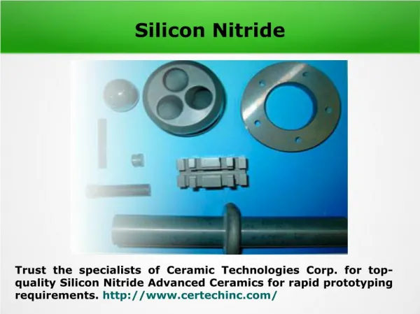
University of the Western Cape. A. Adams and C. J. Arendse. Low temperature deposition of silicon nitride thin films by hot-wire CVD. Energy Postgraduate Conference 2013. Outline. Introduction Experimental Details Results Conclusion Acknowledgments. Introduction. Solar power

E N D
University of the Western Cape A. Adams and C. J. Arendse Low temperature deposition of silicon nitride thin films by hot-wire CVD Energy Postgraduate Conference 2013
Outline • Introduction • Experimental Details • Results • Conclusion • Acknowledgments
Introduction • Solar power • Energy crises • Viable alternative • Amorphous solar cells • Antireflective coating for increased efficiency • Multitude of uses stemming from stoichiometric tunability • Permeation barrier • Gate insulator in thin film electronics • Passivation of dangling bonds • Antireflective coating Deposition Method • Current technique of choice is PECVD • Ion bombardment, resulting in oxidation • Complex (potential difference, plasma source) • Desired technique of choice is HWCVD • Ease of upscale • Eradicates bombardment (absence of plasma ions) • Low cost • High deposition rates of > 7 nm/s • Low temperature deposition
Experimental details • The a-SiN:H thin films were deposited at Tw=1400 °C, Ts = 240 °C, P = 100 µbar, ΦH2 = 20 sccm, ΦSiH4 = 5 sccm and ΦNH3 = 1 – 7 sccm (LOW PARAMETERS)
Results and discussion Decrease in deposition rate as ΦNH3 is increased Competing reaction at the filament Decrease in surface roughness as ΦNH3 is increased columnar structures decreases
Results and Discussion Films are uniform Negligible oxidation occurred in the bulk Increase in N content as NH3 is increased ToF-HIERD and EDS corroborate well NH3 = 5 sccm
Results and discussion Linear relation between static refractive index and N content Direct relation between Tauc band gap and N content
Conclusion • High quality a-SiN:H deposited at low processing parameters, suitable for device applications (permeation barrier, Passivation layer) • Resistant to oxidation • Tuneable refractive index • Corroboration between EDS, ToF-HIERD • Low H content • Silicon rich Films Future Work • Incorporation in organic PV devices
Acknowledgments • Financial Support • University of the Western Cape • National Research Foundation (NRF) • Team • A. Adams, Prof. C. Arendse, Dr. T. F. G. Muller, Dr. G. Malgas, Dr. C. Oliphant and Dr. M. Msimanga.