Download
1 / 15
160 likes | 173 Views
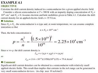
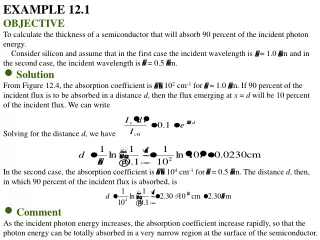
EXAMPLE 3.1 OBJECTIVE Calculate the probability that an energy state in the conduction band at E = E c + kT is occupied by an electron and calculate the thermal equilibrium electron concentration in silicon at T = 300 K.

E N D
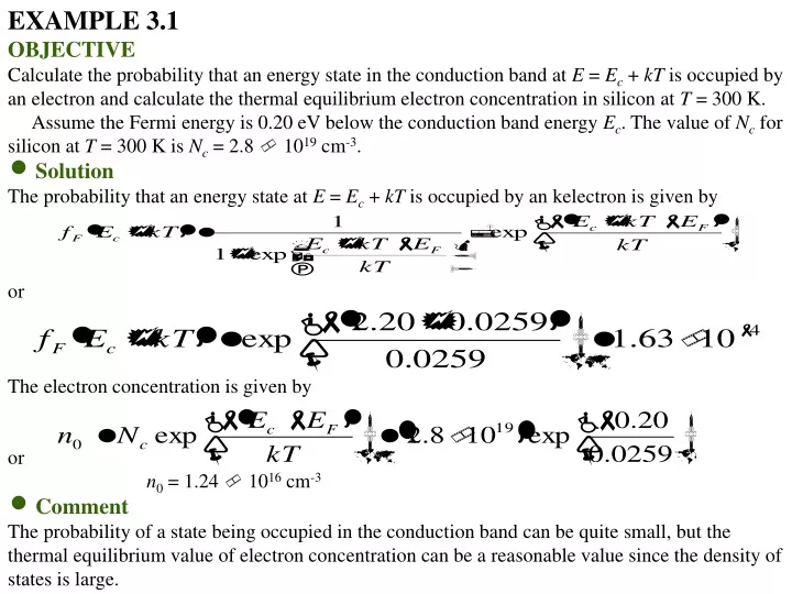
EXAMPLE 3.1 • OBJECTIVE • Calculate the probability that an energy state in the conduction band at E = Ec + kT is occupied by an electron and calculate the thermal equilibrium electron concentration in silicon at T = 300 K. • Assume the Fermi energy is 0.20 eV below the conduction band energy Ec. The value of Nc for silicon at T = 300 K is Nc= 2.8 1019 cm-3. • Solution The probability that an energy state at E = Ec + kT is occupied by an kelectron is given by or The electron concentration is given by or n0 = 1.24 1016 cm-3 • Comment • The probability of a state being occupied in the conduction band can be quite small, but the thermal equilibrium value of electron concentration can be a reasonable value since the density of states is large.
EXAMPLE 3.2 • OBJECTIVE • Calculate the probability that an energy state in the valence band at E = Ev - kT is empty of an electron and calculate the thermal-equilibrium hole concentration in silicon at T = 350 K. • Assume the Fermi energy is 0.25 eV above the valence-band energy. The value of Nv for silicon at T = 300 K is Nv =1.04 1019 cm-3. • Solution The parameter values at T = 350 K are found as and The probability that an energy state at E = Ev – kT is empty is given by or The hole concentration is or p0 = 3.33 1015 cm-3 • Comment The parameter values at any temperature can easily be found using the 300 K values and the temperature dependence of the parameter.
EXAMPLE 3.3 • OBJECTIVE • Calculate the intrinsic carrier concentration in silicon at T = 350 K and at T = 400 K. • The values of Nc and Nv vary as T3/2. As a first approximation, neglect any variation of bandgap energy with temperature. Assume that the bandgap energy of silicon is 1.12 eV. The value of kT at 350 K is • And the value of kT at 400 K is • Solution Using Equation (3.23), we find for T = 350 K so that ni (350 K) = 1.90 1011 cm-3 For T = 400 K, we find so that ni (400 K) = 2.34 1012 cm-3 • Comment • We can note from this example that the intrinsic carrier concentration increases by approximately one order of magnitude for each increase in temperature of 50C.
EXAMPLE 3.4 • OBJECTIVE • Determine the position of the intrinsic Fermi level with respect to the center of the bandgap in silicon at T = 300 K. • The density of states effective mass of the electron is mn* = 1.08m0 and that of the hole is mp* = 0.56m0. • Solution The intrinsic Fermi level with respect to the center of the bandgap is or EFi Emidgap = -12.8 meV • Comment For silicon, the intrinsic Fermi level is 12.8 meV below the midgap energy. If we compare 12.8 meV to 560 meV, which is one-half of the bandgap energy of silicon, we can, in many applications, simply approximate the intrinsic Fermi level to be in the center of the bandgap.
EXAMPLE 3.5 • OBJECTIVE • Calculate the thermal equilibrium concentrations of electrons and holes for a given Fermi energy. • Consider silicon at T = 300 K. Assume that the Fermi level is 0.25 eV above the valence-band energy. If we assume the bandgap energy of silicon is 1.12 eV, then the Fermi energy will be 0.87 below the conduction-band energy. • Solution Using Equation (3.19), we can write Using Equation (3.11),we can write • Comment • The change in the Fermi level is a function of the donor and acceptor impurity concentrations that are added to the semiconductor. This example shows that electron and hole concentrations.
EXAMPLE 3.6 • OBJECTIVE • Determine the hole concentration in silicon at T = 300 K given the electron concentration. • Assume the electron concentration is n0 = 1 1016 cm-3. • Solution From Equation (3.43), we can write or p0 = 2.25 104 cm-3 • Comment • As we have seen previously, the concentrations of electrons and holes can vary by orders of magnitude. The charge carrier that has the greater concentration is referred to as the majority carrier, and the charge carrier that has the lesser concentration is referred to as the minority carrier. In this example, the electron is the majority carrier and the hole is the minority carrier. • The fundamental semiconductor equation given by Equation (3.43) will prove to be extremely useful throughout the remainder of the text.
EXAMPLE 3.7 • OBJECTIVE • Determine the electron concentration using the Fermi-Dirac integral. • Assume that F = 3, which means that the Fermi energy is above the conduction-band energy by approximately 77.7 meV at 300K. • Solution Equation (3.46) can be written as From Figure 3.10, the Fermi-Dirac integral has a value of F1/2(3) 4. Then • Comment • Note that if we had used Equation (3.11), the thermal-equilibrium value of the electron concentration would be n0 = 5.62 1020 cm-3, which is a factor of approximately 4.5 too large. When the Fermi level is in the conduction band, the Boltzmann approximation is no longer valid so that Equation (3.11) is no longer valid.
EXAMPLE 3.8 • OBJECTIVE • Determine the fraction of total electrons still in the donor states at T = 300 K. • Assume silicon is doped with phosphorus to a concentration of Nd = 5 1015 cm-3. • Solution Using Equation (3.55), we fine • Comment • This example shows that the vast majority of the donor electrons are in the conduction band and, in this case, only approximately 0.2 percent of the donor electrons are still in the donor states. For this reason, at room temperature, we can say that the donor states are completely ionized.
EXAMPLE 3.9 • OBJECTIVE • Determine the temperature at which 90 percent of acceptor atoms are ionized. • Consider p-type silicon doped with boron at a concentration of Na = 1016 cm-3. • Solution Find the ratio of holes in the acceptor state to the total number of holes in the valence band plus acceptor state. Taking into account the Boltzmann approximation and assuming the degeneracy factor is g = 4, we write For 90 percent ionization, Using trial and error, we find that T = 193 K. • Comment • This example shows that at approximately 100C below room temperature, we still have 90 percent of the acceptor atoms ionized; in other words, 90 percent of the acceptor atoms have “donated” a hole to the valence band.
EXAMPLE 3.10 • OBJECTIVE • Determine the thermal-equilibrium electron and hole concentrations for a given doping concentration. • Consider silicon at 300 K doped with phosphorus impurity atoms at a concentration of Nd = 2 1016 cm-3. Assume Na = 0. • Solution From Equation (3.60), the majority-carrier electron concentration is The minority-carrier hole concentration is found as • Comment • In this example, Nd >> ni so that the thermal-equilibrium majority-carrier electron concentration is essentially equal to the donor impurity concentration. This example illustrates the fact that we can control the concentration of majority carriers and thus the conductivity of the semiconductor by controlling the concentration of impurity atoms added to the semiconductor material.
EXAMPLE 3.11 • OBJECTIVE • Calculate the thermal-equilibrium electron and hole concentrations in a germanium sample for a given doping density. • Consider a germanium sample at T = 300 K in which Nd = 5 1013 cm-3 and Na = 0. Assume that ni = 2.4 1013 cm-3. • Solution Again, from Equation (3.60), the majority-carrier electron concentration is The minority-carrier hole concentration is • Comment • If the donor impurity concentration is not too different in magnitude from the intrinsic carrier concentration, then the thermal-equilibrium majority carrier electron concentration is influenced by the intrinsic concentration.
EXAMPLE 3.12 • OBJECTIVE • Calculate the thermal-equilibrium electron and hole concentrations in a compensated p-type semiconductor. • Consider a silicon semiconductor at T = 300 K in which the impurity doping concentrations Na = 2 1016 cm-3 and Nd = 5 1015 cm-3. • Solution Since Na > Nd, the compensated semiconductor is p type and the thermal-equilibrium majority-carrier hole concentration is given by Equation (3.62), so that Which yields p0 = 1.5 1016 cm-3 The minority-carrier electron concentration is found to be Comment • If we assume complete ionization and if (Na Nd) >> ni then .the majority-carrier hole concentration is, to a very good approximation, just the difference between the acceptor and donor impurity concentrations.
EXAMPLE 3.13 • OBJECTIVE • Determine the required impurity doping concentration in a semiconductor material. • A silicon power device with n-type material is to be operated at T = 475 K. At this temperature, the intrinsic carrier concentration must contribute no more than 3 percent of the total electron concentration. Determine the minimum doping concentration required to meet this specification. (As a first approximation, neglect the variation of Eg with temperature.) • Solution At T = 475 K, the intrinsic carrier concentration is found from or ni2 = 1.59 1027 which yields ni =3.99 1013 cm-3 For the intrinsic carrier concentration to contribute no more than 3 percent of the total electron concentration, we set n0 = 1.03Nd. From Equation (3.60), we have or which yields Nd = 2.27 1014 cm-3 • Comment • If the temperature remains less than or equal to 475 K, or if the impurity doping concentration is greater than 2.27 1014 cm-3, then the intrinsic carrier concentration will contribute less than 3 percent of the total electron concentration.
EXAMPLE 3.14 • OBJECTIVE • Determine the required donor impurity concentration to obtain a specified Fermi energy. • Silicon at T = 300 K contains an acceptor impurity concentration of Na = 1016 cm-3. Determine the concentration of donor impurity atoms that must be added so that the silicon is n type and the Fermi energy is 0.20 eV below the conduction-band edge. • Solution From Equation (3.64), we have which can be rewritten as Then or Nd = 1.24 1016 + Nd = 2.24 1016 cm-3 • Comment • A compensated semiconductor can be fabricated to provide a specific Fermi energy level.
EXAMPLE 3.15 • OBJECTIVE • Determine the Fermi-level position and the maximum doping at which the Boltzmann approximation is still valid. • Consider p-type silicon, at T = 300 K, doped with boron. We can assume that the limit of the Boltzmann approximation occurs when EF Ev =3 kT (See Section 3.1.2.) • Solution From Table 3.3, we find the ionization energy is Ea Ev = 0.045 eV for boron in silicon. If we assume that EFi >> Emidgap, then from Equation (3.68), the position of the Fermi level at the maximum doping is given by or We can then solve for the doping as • Comment • If the acceptor (or donor) concentration in silicon is greater than approximately 3 1017 cm-3, then the Boltzmann approximation of the distribution function becomes less valid and the equations for the Fermi-level position are no longer quite as accurate.