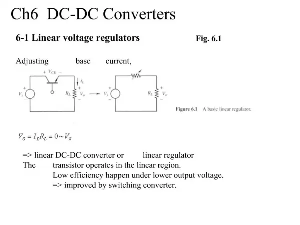
Download
1 / 25
260 likes | 376 Views
Integration Aspects of DC-DC Converters. Katja Klein 1. Physikalisches Institut B RWTH Aachen University. TUPO, June 10 th , 2009. Outline. Conversion ratio & output current Dimensions and weight of buck converters Material budget Cooling requirements Shielding requirements

E N D
Integration Aspects of DC-DC Converters Katja Klein 1. Physikalisches Institut B RWTH Aachen University TUPO, June 10th, 2009
Outline • Conversion ratio & output current • Dimensions and weight of buck converters • Material budget • Cooling requirements • Shielding requirements • Should the DC-DC converter be part of the module? • Possibility of integration for various module proposals • Provision of two operation voltages for CBC • Discussion of four options • Conclusion & recommendation Assumption: GBT powered from outside of sensitive volume
Comparison of Layouts All power numbers include a DC-DC efficiency of 80% § Variant with 2 long barrel pT layers and tracking-only endcaps $ assuming 10Gb/s GBT-like link, 2W per link & with 2W/GBT ° depends on optical module (GBT vs. MZM), larger number for GBT (3W per GBT) * for A = 85cm2 # depends strongly on module proposal
Total Power Consumption • Total power consumption limited by heating up of water-cooled cable channels • Today the total current in cable channels is 15kA • Upper limit would have to be determined by measurements on mock-ups of hot spots in cable channel (Hans Postema) • 10-20% more might be possible, but probably not more? (Hans Postema) • Can calculate maximum power consumption for certain convertion ratio r = Iin / Iout: E.g. for r = 1/10 and 80% efficiency: Pmax = 150kA x 1.2V x 0.8 = 144kW • Can estimate the necessary conversion ratio for a given power consumption: r = 15kA / Iout P = Uout x Iout (includes already converter efficiency of 80%) r = 15kA x Uout /P
Conversion Ratio from Cable Specs • Assume only 1 000 LICs can be used to power the modules (reason: links) • Spec of LICs: Umax = 30V, Imax = 20A (return) • Calculate mean number of modules per LIC • Calculate mean current per LIC • Estimate necessary conversion ratio • In reality, could try to level out (but then granularity becomes an issue)
First Conclusion • Buck converters are needed at least for trigger layers • Charge pumps are no option for some approaches (max. current ~ 1A) • Currents to be provided too big for a single charge pump per module • Charge pump per chip not feasible (90nm, no space for capacitors, ...) • Discuss in the following the integration of buck converters • Come back to charge pumps later
Dimensions and Weight of Buck PCBs Smallest Aachen PCB (V1): Area: 2.3cm2 Height: 10mm Weight: 1.0g 12mm 19mm Aachen PCB with lowest noise (V3): 12mm Area: 3.2cm2 Height: 10mm Weight: 1.1g 27mm Numbers are without connectors
Dimensions and Weight of Buck PCBs CERN PCB (proposal): INDUCTOR SMD SMD SMD ASIC SMD 1.5-2 cm • Area (currently) needed per buck converter PCB: 2-4cm2 • Some further minimization probably possible (e.g. remove connectors) • But filter capacitors are necessary • Coil must have a certain inductance ( noise) and low DC resistance ( efficiency) 1.5-2 cm
Material Budget • TEC, conversion ratio 1/8, eff. = 80%, current power consumption, 1.2V only (Aachen) • One buck converter per module, located close to module Total MB of: TEC modules TEC Converters TEC electronics & cables: - 29% Original TEC TEC with buck converters r = 1/8 With above assumptions, buck converter close to module saves material(caveat: savings are half due to DC-DC conversion, half due to methodology)
Material Budget Buck converters with r = 1/8,located at petal rim: Buck converters with r = ¼ at petal rim,one charge pump with r = ½ per chip TEC electronics & cables: - 18% TEC electronics & cables: - 24% • Buck converter close to module gives largest saving for TEC • Desirable to repeat study for barrel geometry and two operation voltages
Cooling Requirements • Converter efficiency ~ 80% • Heat to be dissipated ranges from 150mW (outer tracker module with 1 hybrid) to ~ 2W (3D-integrated stacked module, inner layers) • A contact to the cooling system should be foreseen
Shielding Requirements Measurements with solenoid coil (worst case) • Measurements show that shielding the whole converter helps against EMI from coil • Shielding only the coil was not so efficient (reason not completely understood) • New Aachen boards need not be shielded anymore in our system test set-up • Requirements depend strongly on distance to FE-electronics (plus technical details of converter and coil...) • Recommendation at this point: a DC-DC converter on the module should be shielded • 30m of Aluminium worked fine (no improvement with thicker shields) • Details would have to be worked out and tested
Integration of Buck Converter (I) • Arguments for buck converter on separate PCB, close to module: • Very limited space on most proposed hybrids size less critical • Larger distance preferred for EMI anyway (also damping of ripple?) • Converter development completely decoupled from hybrid and module development • No common deadlines, can optimize converter design as needed (even late) • Different hybrids for different module proposals avoid involvement of many groups • PCB could be developed, manifactured and tested standalone • Easier for cooling? (module cooling is difficult enough without converters) • Arguments for buck converter on the module/hybrid: • Less mass (avoid connectors & connection between converter and module) • Power regulation closer to FE-ASICs (only relevant if no LDO) • Could have pluggable PCB on hybrid, but then connectors are needed (mass) • Noise effects can be tested more easily (don‘t need additional PCB)
Outer Tracker Module Proposal 2 x 4-MUX + LCDS driver each output 160Mbit/s TCS I/O PLL DC-DC shielded micro-twisted pairs I/O DC-DC out 2.5V • CBC-power ~ 0.75W per hybrid; i.e. 0.75W or 1.5W per module • Plus DCU, PLL, DC-DC inefficiency, GBT-port, MUX, LCDS-driver • No motherboards • Upper part of hybrid ~ 2.5cm x 1cm, no space for buck on this hybrid • Some space between hybrids; but routing of input & output? • Integration of buck on rod level looks more practical and elegant Sensor HV 8x CBC 2x 128ch wire bonded 40Mbit/s out each 2.5cm DCU Sensor with 4x2.5cm strips 2x 1024 @95um pitch integrated pitch adaptor
Outer Tracker Module Proposal • Indeed the buck converter must be able to provide several Amps (as anyway needed by pT-modules) • Could save material by combining two one-hybrid modules into one unit • Could even consider to power two two-hybrid modules (3W) with one converter • Loose two modules if converter fails • No other drawbacks from power point of view
Vertically Integrated Hybrid Module • 130 or 90nm • Communication through vias in ROC and interposer (3D-integration) • No motherboards • FE-power 4-9W per stacked module • Up to 10A per stacked module • Need at least two buck converters per stack (better more) module needs to be “partitioned“ • No space on module; no hybrid • Modules integrated onto “beams“ • Buck converters must be integrated into beam structure • Shielded space already foreseen • Discussions between Fermilab & Aachen started
Trigger Module (Sandro) • 90nm • Sensor size = 4.8cm x 4.8cm • Hybrid ~ 1cm x 4.8cm • Power per pT-module = 2.6W • I per modul ~ 3A • No space for buck converter (unless hybrid is considerably increased) • Practical issues (fabrication?) • Again, integration into support structure seems more feasible • How would support structure look like? 1 Modul: 1 Chip
Trigger Module (Geoff et al.) data out control in 26mm 80mm • Sensor size ~ 2.6cm x 8.0cm • Hybrid ~ 1cm x 4cm • 130nm • Power per pT-module ~ 1.3W (similar to outer tracker module) • No space for buck converters, unless hybrid is considerably increased
Integration of Buck Converter (II) • There is a tendency to avoid motherboards at all • Outer tracker module, vertically integrated double-stack proposal, others? • This goes hand in hand with rather minimalistic hybrids of a few cm2 • All existing or planned buck converter PCBs need an area of 2 - 4cm2 • Suggestion:a separate buck converter PCB close to the module, e.g. inside the beam (for double-stack approach) or on the rod/stave • converter needs cooling contact – probably not too dificult then • need short power cable between converter PCB and module • Could/should be designed such that it fits with all proposals/applications: • Version with 1.2V and 0.9V for CBC • Version with two (or three) buck converters for very high-power trigger modules • Version with 1.2V and 2.5V for GBT, for PP1 or bulkhead
Provision of two Operating Voltages for CBC • Vana = 1.2V, possibility to have Vdig < Vana (~ 0.9V) • P = 64mW per Chip with 1.2V (26mW analog power, digital power would be halved with U = 0.9V) • Both analog and digital currents ~ 20-30mA per chip • How to provide the two voltages? Options: • Use the two LV conductors in LICs and two separate buck converters • Same conversion ratio for both bucks • Power supplies must provide two voltages • Provide one common input voltage, use two separate buck converters • Different conversion ratios for bucks • Lower power losses than option 1. • Derive Vdig from Vana with linear regulator • Method with lowest efficiency • Derive Vdig from Vana with charge pump (ratio 4:3) • Option with lowest mass and space requirements • Brings us to more general question: do we want to use charge pumps, and how?
Option 1: Only Buck Converters • Conversion in one step • Assume buck converter close to the modules with r = 1/6 or smaller (as needed) • If the necessary conversion ratio can be realized in one step for all proposals must be studied with new ASIC prototypes! (issue of switching losses) • Do not use charge pumps no additional chips on the FE-hybrid or inside CBC • Must find space for 1 or 2 buck converters (as many as operating voltages) either on your module/hybrid or (preferred!) on your support structure • If decided to put buck on support structure, module design can proceed completely independently • Could fit with all proposals • Maximal current per buck converter to be understood, of the order of 4A • Looks tight for double-stack proposal, must find reasonable partitioning
Option 2: Buck + Charge Pump per Module • Could be necessary if conversion ratio cannot be provided in one step • Buck converter with r ¼ close to module; charge pump with r = ½ per module • Is however NOT compatible with any pT-module (due to current requirements) • (Only) Possible useful application: provision of Udig for CBC for one FE-hybrid • conversion ratio 4:3, current ~ 300mA • less material than two buck converters (but not half!) • on cost of higher complexity • Space for buck converter: see option 1 • In addition need space for 1 chip plus capacitors (details to be worked out) • on FE-hybrid • or even on buck PCB? • Such a chip is currently not being developed
Option 3: Buck + Charge Pump On-Chip • Assume charge pump is integrated into read-out ASIC • Concerns raised by Mark: substrate noise, constraints on layout, space for passives • Could be necessary if conversion ratio cannot be provided in one step • Buck converter with r ¼ close to module; charge pump with r = ½ per module • Seems NOT compatible with some pT-modules (technology, space for passives) • Possible useful application: provision of Udig for CBC • conversion ratio 4:3, current ~ 20mA • less material than two buck converters (but not half!) • Alternative: derive both voltages with charge pumps • conversion ratio 1:2 one capacitor per voltage (100nF, 0201?) • need LDO for analogue power • can switch on/off single read-out ASICs • how to power auxiliary ASICs (PLL, MUX, LCDS driver, ...)? • Space for buck converter: see option 1 • In addition need space for capacitor(s) close to CBC on FE-hybrid • Design block for 60mA in 130nm being developed by CERN/Atlas
Option 4: Buck + Sep. Charge Pump per Chip • Assume now separate charge pump chip per readout-ASIC • No substrate noise, no constraints on CBC layout • Space for passives still needed, plus space for charge pump chips • Very small chips to be integrated onto hybrid – possible but cumbersome? • Looks NOT compatible with some pT-modules (technology, space) • Possible useful application: provision of Udig for CBC • conversion ratio 4:3, current ~ 20mA • less material than two buck converters, but more than option 3 • Alternative: derive both voltages with charge pumps • conversion ratio 1:2 one capacitor per voltage (100nF, 0201?) • need LDO for analogue power • can switch on/off single read-out ASICs • Space for buck converter: see option 1 • In addition need space for 1 or 2 chips plus capacitor(s) close to CBC
Conclusion & Recommendation (my opinion) • Buck converters cannot be avoided (but charge pumps can) • No motherboards and no or very small hybrids integrate buck converter onto separate small PCB • Cannot decide today if charge pumps are needed, keep option open • Abandon option 4 (separate charge pump chip per read-out ASIC) • Prepare for option 1 with buck on support structure • Explore and do not exclude options 2 & 3 • Allow some space for charge pump chip plus caps on hybrid • Allow some space for caps close to CBC • Integrate charge pump block offered by CERN group into CBC • in a way that it can be bypassed • would learn a lot about option 3 • this is an opportunity to make real progress!