Download
1 / 5
50 likes | 185 Views
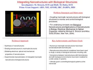
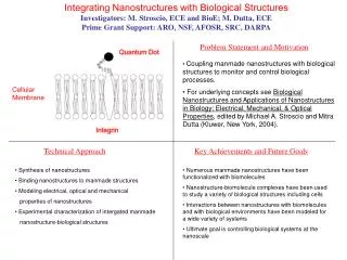
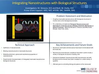
Integrating Nanostructures with Biological Structures Investigators: M. Stroscio, ECE and BioE; M. Dutta, ECE Prime Grant Support: ARO, NSF, AFOSR, SRC, DARPA, DHS. Problem Statement and Motivation.

E N D
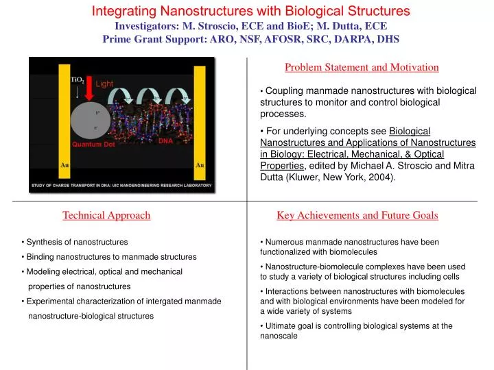
Integrating Nanostructures with Biological Structures Investigators: M. Stroscio, ECE and BioE; M. Dutta, ECE Prime Grant Support: ARO, NSF, AFOSR, SRC, DARPA, DHS Problem Statement and Motivation • Coupling manmade nanostructures with biological structures to monitor and control biological processes. • For underlying concepts see Biological Nanostructures and Applications of Nanostructures in Biology: Electrical, Mechanical, & Optical Properties, edited by Michael A. Stroscio and Mitra Dutta (Kluwer, New York, 2004). Technical Approach Key Achievements and Future Goals • Synthesis of nanostructures • Binding nanostructures to manmade structures • Modeling electrical, optical and mechanical • properties of nanostructures • Experimental characterization of intergated manmade • nanostructure-biological structures • Numerous manmade nanostructures have been functionalized with biomolecules • Nanostructure-biomolecule complexes have been used to study a variety of biological structures including cells • Interactions between nanostructures with biomolecules and with biological environments have been modeled for a wide variety of systems • Ultimate goal is controlling biological systems at the nanoscale
Nano-magnetism and high-density magnetic memory Vitali Metlushko, Department of Electrical & Computer Engineering and Nanotechnology Core Facility (NCF) Prime Grant Support: NSF ECS grant # ECS-0202780, Antidot and Ring Arrays for Magnetic Storage Applications and NSF NIRT grant # DMR-0210519 : Formation and Properties of Spin-Polarized Quantum Dots in Magnetic Semiconductors by Controlled Variation of Magnetic Fields on the Nanoscale, B. Janko (P.I.), J. K. Furdyna (co-P.I.), M. Dobrowolska (co-P.I.), University of Notre Dame is leading organization, A. M. Chang (Purdue) and V. Metlushko, (UIC) SEM image of 700nm MRAM cells. Problem Statement and Motivation Lorentz image of magnetic nanostructure. The field of nanoelectronics is overwhelmingly dedicated to the exploitation of the behavior of electrons in electric fields. Materials employed are nearly always semiconductor-based, such as Si or GaAs, and other related dielectric and conducting materials. An emerging basis for nanoelectronic systems is that of magnetic materials. In the form of magnetic random access memories (MRAM), nanoscale magnetic structures offer fascinating opportunities for the development of low-power and nonvolatile memory elements. UIC’s Nanoscale Core Facility Key Achievements and Future Goals Technical Approach In past few years, the interest in nano-magnetism has encreased rapidly because they offer potential application in MRAM. Modern fabrication techniques allow us to place the magnetic elements so close together that element-element interactions compete with single-element energies and can lead to totally different switching dynamics. To visualize the magnetization reversal process in individual nano-magnets as well as in high-density arrays, Metlushko and his co-authors employed several different imaging techniques- magnetic force microscopy (MFM), scanning Hall microscopy, magneto-optical (MO) microscopy, SEMPA and Lorentz microscopy (LM). • This project has led to collaboration with MSD, CNM and APS ANL, Katholieke Univesiteit Leuven, Belgium, University of Notre Dame, NIST, Universita` di Ferrara, Italy, Inter-University Micro-Electronics Center (IMEC), Belgium, Cornell University, McGill University and University of Alberta, Canada • During the past 3 years this NSF-supported work resulted in 21 articles in refereed journals already published and 10 invited talks in the US, Europe and Japan.
Tera-scale Integration of Semiconductor Nanocrystals Investigators: M. Dutta, ECE; M. Stroscio,ECE and BioE Prime Grant Support: ARO, NSF, AFOSR, SRC, DARPA Au wire CdSe-ZnS-GGGC CdSe-ZnS CdS Problem Statement and Motivation • Future electronic and optoelectronic systems must be integrated on the terascale and beyond • This research effort explores the use of biomolecules as molecular interconnects for such terascale systems Key Achievements and Future Goals Technical Approach • Numerous manmade semiconducting nanostructures have been synthesized • Integrated semiconductor quantum dots have been assembled chemically in the Nanoengineering Research Laboratory at UIC • Interactions between semiconductor nanostructures and molecular wires have been modeled for a wide variety of systems • Untimate goal is massive integration of semiconductor nanostructures in functional electronic and optoelectronic networks • Synthesis of semiconductor nanostructures • Chemical self-assembly of semiconductor • nanostructures • Modeling electrical, optical and mechanical • properties of ensembles of nanostructures • Experimental characterization of massively integrated • networks of semiconductor nanostructures
Multiferroic Thin Films Grown by MBE Investigators: Siddhartha Ghosh Prime Grant Support: Office of Naval Research Problem Statement and Motivation • Frequency tunable microwave devices • Magnetoelectric thin films • Multiferroism in multilayered heterostructures • Advanced RADAR arrays for Navy • Spintronics Key Achievements and Future Goals RF Plasma Assisted Oxide MBE System • First reported MBE growth of multiferroic layers by RF Plasma oxygen source • Research on controlling thin film interfaces is underway • Collaboration has been established with Argonne National Labs and Center for Nanoscale Materials • Discussion for collaboration with Naval Research Laboratory has been initiated Technical Approach • RF Plasma assisted complex oxide epitaxial • growth on oxide and semiconductor substr- • ates • Alternate piezoelectric and magnetostrictive layers provide mechanical coupling between the ferroelectric and ferromagnetic thin films • Atomically smooth interfaces
MicroOptoElectroMechanical Systems (MOEMS) Investigators: A. Feinerman, ECE; C. Megaridis, MIE Prime Grant Support: NASA, and DARPA Problem Statement and Motivation • Standard deformable structures rely on spindly linkages to achieve the flexibility required for motion. • Spindly structures are thermal insulators. • Tethered liquid drops provide electrical, and thermal conduction, as well as a restoring force/torque to mirror. 75 volts @ 300Hz with 35 mm actuation Key Achievements and Future Goals Technical Approach • tethered drops are super-deformable, large displacements at low voltages are possible • drops can be tethered by patterning the wetting properties of a surface • precision dispensing of Hg drops • self-alignment of ~50 mg mirrors. • Achieved reproducible piston motion • Achieved reproducible rotation • Used technique to make variable reflection display • Developing RF switch – liquids do not suffer from stiction.