Download
1 / 2
20 likes | 25 Views
Every PCB or printed circuit board uses traces of copper in the core and the layers. This metal is present even on the outermost layers as the primary component. According to the experts of a China PCB Supplier Company, inconsistent distribution of this element while stacking up the layers can lead to several problems, including warpage, twisting, and bowing.

E N D
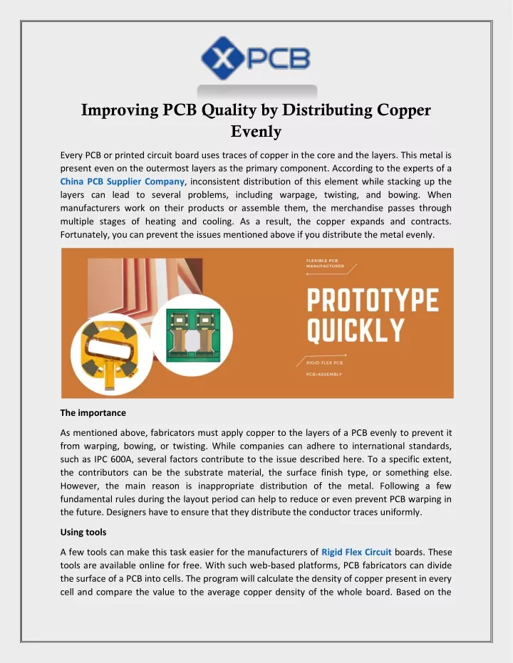
Improving PCB Quality by Distributing Copper Evenly Every PCB or printed circuit board uses traces of copper in the core and the layers. This metal is present even on the outermost layers as the primary component. According to the experts of a China PCB Supplier Company, inconsistent distribution of this element while stacking up the layers can lead to several problems, including warpage, twisting, and bowing. When manufacturers work on their products or assemble them, the merchandise passes through multiple stages of heating and cooling. As a result, the copper expands and contracts. Fortunately, you can prevent the issues mentioned above if you distribute the metal evenly. The importance As mentioned above, fabricators must apply copper to the layers of a PCB evenly to prevent it from warping, bowing, or twisting. While companies can adhere to international standards, such as IPC 600A, several factors contribute to the issue described here. To a specific extent, the contributors can be the substrate material, the surface finish type, or something else. However, the main reason is inappropriate distribution of the metal. Following a few fundamental rules during the layout period can help to reduce or even prevent PCB warping in the future. Designers have to ensure that they distribute the conductor traces uniformly. Using tools A few tools can make this task easier for the manufacturers of Rigid Flex Circuit boards. These tools are available online for free. With such web-based platforms, PCB fabricators can divide the surface of a PCB into cells. The program will calculate the density of copper present in every cell and compare the value to the average copper density of the whole board. Based on the
information, it will assign a color to each cell. The ones marked in blue will tell the manufacturers that the copper isn’t evenly distributed there. On the other hand, the red color will inform them that they’ve used more copper than necessary. Copper thieving Manufacturers often add copper thieving to their products. They do this as a DFM procedure that indicates an uneven copper distribution on the board. Their primary objective is to adjust the copper distribution across a layer to add uniformity. It facilitates more predictability during plating and etching. As this process requires the fabricators to submerge the copper cladding into a chemical bath, the areas will varying metal densities will have various rates during etching and plating. The ultimate objective of ensuring the even distribution of copper is to augment the quality and reliability of the product. Contact Us: Address: Building 3, JinFeng Industry Area, Heping Community, Fuyong Town, Baoan District, Shenzhen, 518103, China Phone: +8616675561662 E-mail:Xpcb.limited@gmail.com Website: https://www.x-pcb.com Source: https://xpcbcn.livejournal.com/2196.html