Download
1 / 60
660 likes | 1.32k Views
IL 2222 - MOSFET. Professor Ahmed Hemani Dept. Of ES, School of ICT, KTH Kista Email: hemani@kth.se Website: www.it.kth.se/~hemani. MOS Capacitor, MOSFET. MOS: M etal- O xide- S emiconductor. ~1.5nm thick Few oxide molecules Usually made of Poly Silicon. V g. V g. gate. gate. metal.

E N D
IL 2222 - MOSFET Professor Ahmed Hemani Dept. Of ES, School of ICT, KTH Kista Email: hemani@kth.se Website: www.it.kth.se/~hemani
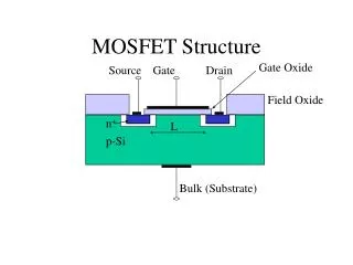
MOS Capacitor, MOSFET MOS: Metal-Oxide-Semiconductor ~1.5nm thick Few oxide molecules Usually made of Poly Silicon Vg Vg gate gate metal SiO2 SiO2 N+ N+ P-body Si body MOS transistor MOS capacitor Modern Semiconductor Devices for Integrated Circuits (C. Hu)
Surface Accumulation Fsis neglible in accumulation fs : surface potential, band bending Vox: voltage across the oxide Make Vg < Vfb
Surface Depletion Modern Semiconductor Devices for Integrated Circuits (C. Hu)
Threshold Condition and Threshold Voltage Threshold (of inversion): ns = Na, or (Ec–Ef)surface= (Ef–Ev)bulk , or A = B, and C = D Modern Semiconductor Devices for Integrated Circuits (C. Hu)
Threshold Voltage At threshold, Modern Semiconductor Devices for Integrated Circuits (C. Hu)
+ for P-body, – for N-body Threshold Voltage
Inversion Layer Charge, Qinv (C/cm2) Modern Semiconductor Devices for Integrated Circuits (C. Hu)
Choice of Vtand Gate Doping Type Vt is generally set at a small positive value So that, at Vg = 0, the transistor does not have an inversion layer and current does not flow between the two N+regions. Enhancement type device • P-body is normally paired with N+-gate to achieve a small positive threshold voltage. • N-body is normally paired with P+-gate to achieve a small negative threshold voltage. Modern Semiconductor Devices for Integrated Circuits (C. Hu)
Review : Basic MOS Capacitor Theory Modern Semiconductor Devices for Integrated Circuits (C. Hu)
total substrate charge, Qs Review : Basic MOS Capacitor Theory Modern Semiconductor Devices for Integrated Circuits (C. Hu)
MOS CV Characteristics Modern Semiconductor Devices for Integrated Circuits (C. Hu)
MOS CV Characteristics The quasi-static CV is obtained by the application of a slow linear-ramp voltage (< 0.1V/s) to the gate, while measuring Ig with a very sensitive DC ammeter. C is calculated from Ig = C·dVg/dt. This allows sufficient time for Qinv to respond to the slow-changing Vg. Modern Semiconductor Devices for Integrated Circuits (C. Hu)
Equivalent circuit in the depletion and the inversion regimes (d) (a) (c) (b) General case for both depletion and inversion regions. In the depletion regions VgVt Strong inversion Modern Semiconductor Devices for Integrated Circuits (C. Hu)
MOSFET • The MOSFET (MOS Field-Effect Transistor) is the building block of Gb memory chips, GHz microprocessors, analog, and RF circuits. • MOSFET the following characteristics: • small size • high speed • low power • high gain Modern Semiconductor Devices for Integrated Circuits (C. Hu)
Introduction to the MOSFET Basic MOSFET structure and IV characteristics Modern Semiconductor Devices for Integrated Circuits (C. Hu)
Introduction to the MOSFET Two ways of representing a MOSFET: Modern Semiconductor Devices for Integrated Circuits (C. Hu)
Complementary MOSFETs Technology Modern Semiconductor Devices for Integrated Circuits (C. Hu)
CMOS (Complementary MOS) Inverter Modern Semiconductor Devices for Integrated Circuits (C. Hu)
MOSFET Vt and the Body Effect Two capacitors => two charge components • RedefineVtas Modern Semiconductor Devices for Integrated Circuits (C. Hu)
Body effect:Vtis a function ofVsb. When the source-body junction is reverse-biased, Vtincreases. • Body effect coefficient: • a = Cdep/Coxe • = 3Toxe / Wdep MOSFET Vt and the Body Effect Body effect slows down circuits? How can it be reduced? Modern Semiconductor Devices for Integrated Circuits (C. Hu)
Retrograde Body Doping Profiles Wdmax for retrograde doping Wdmax for uniform doping • Wdepdoes not vary withVsb. • Retrograde doping is popular because it reduces off-state • leakage and allows higher surface mobility. Modern Semiconductor Devices for Integrated Circuits (C. Hu)
Uniform Body Doping When the source/body junction is reverse-biased, there are two quasi-Fermi levels (Efn and Efp) which are separated by qVsb. An NMOSFET reaches threshold of inversion when Ec is close to Efn, not Efp. This requires the band-bending to be 2fB + Vsb, not 2fB. g is the body-effect parameter. Modern Semiconductor Devices for Integrated Circuits (C. Hu)
Channel voltage Vcs (x) x = 0:Vcs= Vs x = L: Vcs= Vd Qinv in MOSFET • Qinv= – Coxe(Vgs– Vcs– Vt0 – a (Vsb+Vcs) • = – Coxe(Vgs– Vcs– (Vt0 + a Vsb) – a Vcs) • = – Coxe(Vgs – mVcs – Vt) • m º 1 +a = 1 + 3Toxe/Wdmax • m is called the bulk-charge factor • Typically m is 1.2 but can be simplified to 1 Modern Semiconductor Devices for Integrated Circuits (C. Hu)
How to Measure the Vt of a MOSFET ? A B • Method A. Vt is measured by extrapolating the Ids versus Vgs curve to Ids = 0. • Method B. The Vg at which Ids =0.1mA W/L Modern Semiconductor Devices for Integrated Circuits (C. Hu)
Basic MOSFET IV Model Ids= WQinvv= WQinvmnE = WCox(Vgs– mVcs–Vt)mndVcs/dx IdsL = WCoxmn(Vgs– Vt– mVds/2)Vds Process Transconductance Gain factor m is typically 1.2 but can be simplified to 1 Modern Semiconductor Devices for Integrated Circuits (C. Hu)
Vdsat : Drain Saturation Voltage Modern Semiconductor Devices for Integrated Circuits (C. Hu)
Saturation Current and Transconductance Drain current in saturation region Transconductance: gm= dIds/dVgs Modern Semiconductor Devices for Integrated Circuits (C. Hu)
Saturation – Pinch Off Modern Semiconductor Devices for Integrated Circuits (C. Hu)
Channel Length Modulation • Increasing the Vds has the effect of the reducing the channel length as the depletion region on the drain side increases. • Channel length reduction lower resistance Increase in Drain Current • More pronounced for short channels • One of the five short channel effects
m E = n v E + 1 E sat 5 E<<Esat: v = mE u = 10 sat n E>>Esat: v = m Esat ) n s / m ( n u x = 1.5 x (V/µm) c Velocity Saturation Constant velocity Constant mobility (slope = µ) • Velocity saturation has large and deleterious effect on the Ionof MOSFETS Modern Semiconductor Devices for Integrated Circuits (C. Hu)
= I WQ v ds inv m dV / dx = - - ns cs I WC ( V mV V ) ds oxe gs cs t dV + 1 cs / E sat dx L V ò ò = m - - - ds I dx [ WC ( V mV V ) I / ] dV E ds oxe ns gs cs t ds sat cs 0 0 m = m - - - I L WC ( V V V ) V I V / E sat ds oxe ns gs t ds ds ds ds 2 MOSFET IV Model with Velocity Saturation Vcs /L– the average electric field is replaced by Modern Semiconductor Devices for Integrated Circuits (C. Hu)
W m m - - C ( V V V ) V oxe ns gs t ds ds L 2 = I ds V + 1 ds L E sat long - channel I ds = I ds + 1 V / L E sat ds MOSFET IV Model with Velocity Saturation Modern Semiconductor Devices for Integrated Circuits (C. Hu)
dI = ds Solving 0 , dV ds - 2 ( V V ) / m gs t = V dsat + + - 1 1 2 ( V V ) / mE L sat gs t 1 m 1 = + - V V V L E sat dsat gs t MOSFET IV Model with Velocity Saturation A simpler and more accurate Vdsatis: 2 v º dsat E sat m ns Modern Semiconductor Devices for Integrated Circuits (C. Hu)
- 1 æ ö m 1 ç | = + V ç | dsat - V V L E è ø sat gs t EXAMPLE: Drain Saturation Voltage Question: At Vgs = 1.8 V, what is the Vdsat of an NFET with Toxe= 3 nm, Vt= 0.25 V, and Wdmax = 45 nm for (a) L =10 mm, (b) L = 1 um, (c) L = 0.1 mm, and (d) L = 0.05 mm? Solution:From Vgs, Vt, and Toxe, mns is 200 cm2V-1s-1. Esat= 2vsat/m ns = 8 104V/cm m = 1 +3Toxe/Wdmax = 1.2 Modern Semiconductor Devices for Integrated Circuits (C. Hu)
- 1 æ ö m 1 | ç = + V | ç dsat - V V L E è ø sat gs t EXAMPLE: Drain Saturation Voltage (a) L = 10 mm, Vdsat= (1/1.3V + 1/80V)-1 = 1.3 V (b) L = 1 mm, Vdsat= (1/1.3V + 1/8V)-1 = 1.1 V (c) L = 0.1 mm, Vdsat= (1/1.3V + 1/.8V)-1 = 0.5 V (d) L = 0.05 mm, Vdsat= (1/1.3V + 1/.4V)-1 = 0.3 V Modern Semiconductor Devices for Integrated Circuits (C. Hu)
- 2 long - channel I ( V V ) W dsat gs t = m = I C - - dsat ox s V V V V 2 mL gs t gs t + + 1 1 L L mE mE sat sat << - L V V E sat gs t = - - I Wv C ( V V L ) mE = - I Wv C ( V V ) dsat sat sat ox gs t dsat sat ox gs t Idsat with Velocity Saturation Substituting Vdsat for Vds in Ids equation gives: Very short channel case: Idsatis proportional toVgs–Vtrather than(Vgs– Vt)2 , not as sensitive to L Modern Semiconductor Devices for Integrated Circuits (C. Hu)
-4 x 10 6 VGS= 2.5 V 5 Resistive Saturation 4 VGS= 2.0 V Quadratic Relationship (A) 3 VDS = VGS - VT D I 2 VGS= 1.5 V 1 VGS= 1.0 V 0 0 0.5 1 1.5 2 2.5 V (V) DS Current-Voltage RelationsA good ol’ transistor
Velocity Saturation The IDSAT in short Channel Device has linear dependence on VGS as opposed to square dependence thus significantly reducing the drain current delivered for a given voltage and thus slows down the device I D Long-channel device V = V GS DD Short-channel device V V - V V DSAT GS T DS The Short Channel Device enters saturation before VDS > VGS - VT
Velocity Saturation What is the main difference between the Vg dependence of the long- and short-channel length IV curves? Modern Semiconductor Devices for Integrated Circuits (C. Hu)
-2 10 Linear -4 10 -6 Quadratic 10 (A) D I -8 10 Exponential -10 10 VT -12 10 0 0.5 1 1.5 2 2.5 V (V) GS Sub-Threshold Conduction The Slope Factor S is DVGS for ID2/ID1 =10 Typical values for S: 60 .. 100 mV/decade
-4 x 10 2.5 VDS=VDSAT 2 G VelocitySaturated 1.5 Linear S D 1 VDSAT=VGT B 0.5 VDS=VGT Saturated 0 0 0.5 1 1.5 2 2.5 A Unified Model (A) D I V (V) DS