Download

1 / 55
600 likes | 895 Views
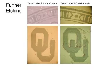
ETCHING. WAFER PROCESS FLOW. DEFINITION. Patterned Etch. Blanket Etch. HISTORY. Adopted in semiconductor industry for transistor & IC manufacture in 1950’s Before 1980, chemical solution were used to dissolve the materials not covered by PR to achieve the pattern transfer

E N D
Patterned Etch Blanket Etch
HISTORY • Adopted in semiconductor industry for transistor & IC manufacture in 1950’s • Before 1980, chemical solution were used to dissolve the materials not covered by PR to achieve the pattern transfer • After 1980, replaced by dry (plasma) etch processes