Download
1 / 15
160 likes | 527 Views
FYS0460 / FYSZ460 Advanced Laboratory Exercise Electron Beam Lithography. Terhi Hongisto terhi.hongisto@jyu.fi YN240. The Objective of the Laboratory Exercise. To give an introduction to The operation of a S canning E lectron M icroscope (SEM) E lectron B eam L ithography (EBL)

E N D
FYS0460 / FYSZ460Advanced Laboratory ExerciseElectron Beam Lithography Terhi Hongisto terhi.hongisto@jyu.fi YN240
The Objective of the Laboratory Exercise To give an introduction to • The operation of a Scanning Electron Microscope (SEM) • Electron Beam Lithography (EBL) • Working in laboratory and in cleanroom conditions
About electron microscopes • The light used in optical microscopes is ‘substituted’ with very thin beam of electrons → smaller wave lenght → better resolution SEM: conducting samples TEM: (transmission electron microscope) the samples have to be thin enough for the electrons to transmitt • Operated in vacuum → less scattering of the electrons →only for solid state samples (e.g. biological samples have to be dryed and coated) Kuva: SEM/TEM/Optical
About the interaction of the electron beam and the sample • Different interactions → depending both on the sample and the detector different kind of information obtained →information from the different layers of the sample →different kind of detectors needed Kuva: vuorovaikutukset
About the interaction of the electron beam and the sample • Secondary electrons number of SEs strongly dependent on the incident angle, low energy → surface topography • Backscattered electrons energy much higher, the number and the scattering direction of BEs determined by the incident angle and the atomic number of the substanses composing the specimen surface
Magnification • Electron beam scanned over the sample • Information emitted from each scanned point • The signal from the detector (e.g. the number of SEs) amplified and fed into CRT (cathode-ray tube, nowadays often computer screen) • On the CRT the brightness is controlled according to the signal stength as a function of the position of electron beam on the sample Kuva: Kuvan muodostus
Generation of Electron beam • Filament (W) heated by current (thermionic emission source) • Emitted electrons accelerated by high voltage • e-beam focused by magnetic lenses • Beam scanned over the sample by deflection coils • Scattered (transmitted) electrons detected Kuva: Column
Detectors SE: collected by “post acceleration voltage” applied to scintillator → shadowless illumination image formed BE: semiconductor detector, image formed by the electrons emitted towards the detector → one-side illumination image formed
Features of the SEMs + high resolution + high contrast + high depth of field/focus, large focal depth - charging up effects - aberrations (chromatic, ) - astigmatism - sensitivity to vibrations etc.external factors • Kuva: glomerulus
Lithography UV lithography most commonly used in in industry -fast, parallel exposure -suitable for mass production -commercial products: line width 90 nm (65 nm ?), highly complicated & specified optics required EBL in research -smaller line width -slow(er), serial exposure -flexible -industrial application: mask making for UV lithography
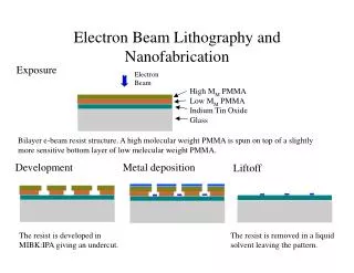
Lithography 2 layer resist: PMMA, PMMA-MAA (=co-polymer)
Resists 2 tasks - to react to radiation - to protect the surface 3 components - film forming - sensitive to the radiation - solvent Positive vs. negative resist
Exposure Induces change in the resist • Optical • Mask required • Parallel • Limiting factors • wave length, diffraction in mask/resist • EBL • Serial, point by point • Limiting factors • resist Dose, cross linking, acceleration voltage, proximity effect (inter-/ intra-)
Developing • Chip immersed to the developer chemical • Exposed resist with smaller molec. Weight dissolves more readily • Undercut profile Other process steps: • Metal coating/deposition • Lift-off
Practical issues • Study material Invitation to the SEM World: ”Dictionary” Error on page 2 • Design Cad • Report • Schedule for the practical part