Download
1 / 22
220 likes | 369 Views
Introduction to Prototyping a LED Driver. Part II: Using PCB Layout Software – Custom Component Libraries. September 24-28, 2012 Carol Lenk. What’s in a Component. Component Connection between pins and pads Values, Component height, Digikey/Mfr part number. Board Symbol

E N D
Introduction to Prototyping a LED Driver Part II: Using PCB Layout Software – Custom Component Libraries September 24-28, 2012Carol Lenk
What’s in a Component • Component • Connection between pins and pads • Values, Component height, Digikey/Mfr part number Board Symbol Pad Footprint: copper, mask Reference Name Silkscreen, Document • Schematic Symbol • Schematic Shape • Pins
HV9910 • Component not in library. • Package is standard. • Schematic symbol is standard. • Need to make a new Component that uses existing SO-8 PCB symbol and schematic symbol.
Find SO-8 PCB Symbol • Library Manager • PCB Symbol Tab • Use All Libraries • Find… • Search for “SO” and 8 pads • Click on 8-SOIC [prolib]
Find SO-8 Schematic Symbol • Library Manager • Schematic Symbol Tab • Use All Libraries • Find… • Search for “SO” and 8 pads • Click on FCH-SO8 [fairchild1]
New Component • Library Manager • Components Tab • New Item…
HV9910 • Assign pins 1 to 1 • Enter Terminal Name • Save to our custom library
Custom Footprint • Download datasheet from Digikey. • Find component size and recommended land pattern.
Custom PCB Symbol Create custom PCB Symbol library • Library Manger • PCB Symbols Tab: New Lib… : 9910Demo.psl • Copy a 2 pad footprint • In prolib.psl, copy SMD1 to custom library • Name new pcb symbol DR1050
Edit Custom PCB Symbol • Library Manager, go to 9910Demo.psl, select DR1050, click Edit • Right click on S (symbol origin) : Origins : Set System Origin at Item • Menu: Units: mm • Double click on pad to bring up Properties • Change position (center of pad) 0.8 4.45 4.45 3.65 X
Menu: Settings: Grids: Step Size 0.1mm. • Double click on corners to add chamfer. • Move R reference locator to outside of body • Pads underneath part makes it hard to hand solder. • Increase pad size by 1 mm.
Library Manager: Component Tab: New Item • Component Editor • Connect Sch Terminals to PCB Pads • Save to custom library • Add Component to schematic.
MOSFET • Add pad numbers • Add description in Properties window.
Diode • Schematic Symbol • Use Diode-2 in diode.ssl library • Need to create custom PCB symbol • Copy pcb symbol “1206” from sm.psl library. • Name new symbol “SMA”
Diode PCB Symbol • With line selected, hit “L” to change layers. • Purple items are on Top Document layer to show components. Layer not printed on PCB. • Yellow items are on Top Silkscreen layer. They are printed on the PCB. • With line selected, hit “s” to change line style thickness. • For closed shape, use Properties and click on Filled.
Footprint Guidelines • Reduce production errors. • Alignment, solderability, inspectable. • IPC Standards. • From datasheets for resistors, capacitors, etc. • Generally ~ 0.005” wider overall, 0.020” longer on each side. • Hand solderable for prototypes.
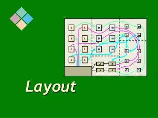
How is a PCB Made? 2 1 3 4
Looking at a PCB White Silkscreen Pin connector Reference Designator on Silkscreen Layer Green Solder Mask Copper Trace visible under solder mask Tinned Pad
Layers • In Interaction Bar (Menu: View or F9), Layers Tab is at bottom. • Hit “c” to bring up colors.