Download
1 / 11
110 likes | 206 Views
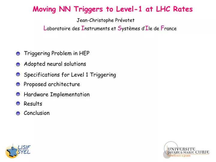
Moving NN Triggers to Level-1 at LHC Rates. Jean-Christophe Prévotet. L aboratoire des I nstruments et S ystèmes d’ I le de F rance. Triggering Problem in HEP. Adopted neural solutions. Specifications for Level 1 Triggering. Proposed architecture. Hardware Implementation. Results.

E N D
Moving NN Triggers to Level-1 at LHC Rates Jean-Christophe Prévotet Laboratoire des Instruments et Systèmes d’Ile de France Triggering Problem in HEP Adopted neural solutions Specifications for Level 1 Triggering Proposed architecture Hardware Implementation Results Conclusion
Triggering problem in High Energy Physics Detector Reject Level 1 Trigger ~1µs Dedicated Hardware Implementation Y~0 Background Y~1 Physics Reject Level 2 Trigger ~20µs Reject Level 3 Trigger Conventional Microprocessors Incoming data from sub-detectors Reject Level 4 Trigger Reject Offline event reconstruction
Hardware Adopted Solutions Current solutions Level 1 Trigger Latency of 500ns => No digital circuits possible OR Straightforward Circuits made of RAMs : lack of precision, small networks Level 2 Trigger Latency of 10µs => Possible use of digital circuits Exple: CNAPS in the H1 experiment => 8µs to execute a 64x64x1 net DSPs Future solutions Technology trend enables to transpose L2 complexity of neural computations into L1
Level 1 Trigger Scheme 500ns Demultiplex unit Neural processing FPGAs Multiplex unit Output data To Level2 (every 25ns) Analog signals from the calorimeter Preprocessor Digitization Pre-Sums, … Main control module Timing Specifications of the ATLAS experiment at LHC Data arrive each BC (25ns) and processed in a time multiplexed way
Specifications Electrons, tau, hadrons, jets 4 64 …….. …….. 128 Execution time : 500 ns with data arriving every BC=25ns Weights coded in 16 bits States coded in 8 bits
Neural processor Architecture Control unit Matrix of n*m Processing Elements (PEs) Control unit PE PE PE PE ACC TanH I/O module PE PE PE PE TanH are stored in LUT ACC TanH 1 matrix row computes a neuron PE PE PE PE The result is back-propagated To calculate the output layer ACC TanH PE PE PE PE ACC TanH 256 PEs for a 128x64x4 network I/O module
PE architecture Data in Data out Multiplier Accumulator Input data 8 + X 16 Weights mem Addr gen Control Module cmd bus
Row Accumulator Input bus (data coming from other rows) Register bank Din 29 32 8 Adder Trunc 8 8 Output bus (data going to other rows) Registers Multiplexers / Demultiplexers Truncation unit
cout y G4 G3 G2 G1 Carry & Control yq D Q LUT xb x F4 F3 F2 F1 Carry & Control xq D Q LUT bx cin Xilinx Virtex slice Hardware Implementation in a FPGA What is a FPGA… I/O Ports Block Rams DLL Programmable Logic Blocks Programmable connections
Results Timing Time in clock cycles for the whole neural net : around 60 cycles. Target Clock frequency Processing time: => VIRTEX2 compatible 120MHz 8.33ns What is done today… Description of the whole design in VHDL Functionnal simulations of the different modules (Multipliers, acc, control, PE..) Individual Modules synthesis (translated into logic blocks) What has to be done… Global synthesis and implementation on the FPGA Timing and resources optimization
Summary Implementation of digital neural network feasible in real time Transposition of level2 concepts into Level 1 Proposed architecture Advantages Flexibility Implementation in a FPGA => easily re-configurable Coding precision easily changeable Weight Precision, activation functions, etc. Processing time: doesn’t really depend on the number of neurons in the hidden layer 1 neuron = 4 added PEs Disadvantages Resources consuming => many FPGAs required Fewer performances than custom circuits