Download
1 / 106
1.1k likes | 1.36k Views
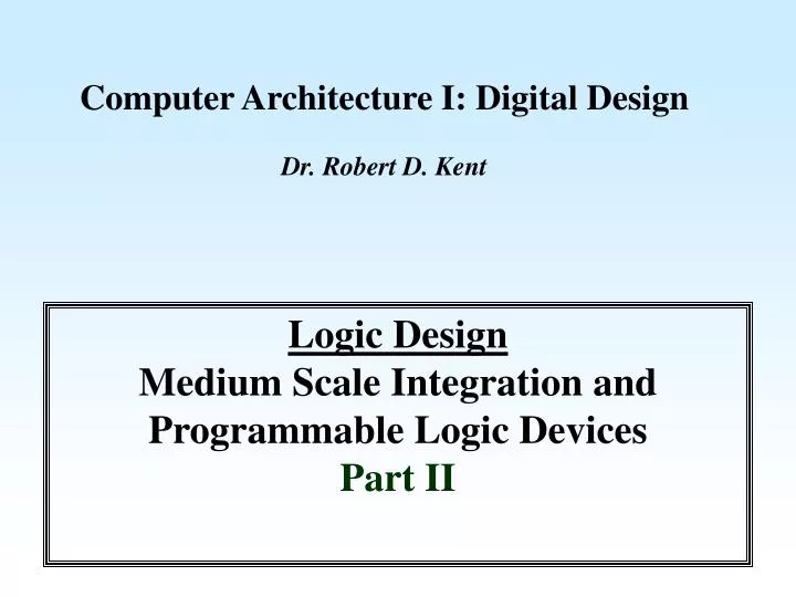
Computer Architecture I: Digital Design Dr. Robert D. Kent. Logic Design Medium Scale Integration and Programmable Logic Devices Part II. Review.

E N D
Computer Architecture I: Digital Design Dr. Robert D. Kent Logic Design Medium Scale Integration and Programmable Logic Devices Part II
Review • At the outset of designing a complex system, such as a modern computer or network, it is clear that design is extraordinarily difficult and computationally challenging when performed at the level of fundamental Boolean logic gates. • For these reasons modern design approaches are based on hierarchical, component based methods. • Leading to simplified, localized component design, • lowering of design costs, • shifting some aspects of design to the component interface (the compatibility problem). • We now continue our study of MSI circuits to better understand this process of MSI design.
Goals • We continue our study of simple, but functional Combinational circuits: • we continue constructing a small library of useful components • through study of the solution process using Boolean algebra and Boolean calculus (simplification, etc.) we better understand the meaning of SSI design • we seek to identify these components for their re-use potential • through our study we will better understand how MSI increases the level of abstraction in solving problems - SSI design is relatively concrete.
Circuit # 4 : Binary Subtractor • Before proceeding to design a subtractor circuit, consider a few examples of the operation D = X - Y: • Example 1 : • Example 1 : • X 0 0 1 1 • Y 0 0 0 1 • ======= • D 0 0 1 0 Considered “easy” because: 1-1 = 0 is easy 1-0 = 1 is easy 0-0 = 0 is easy But .....
Circuit # 4 : Binary Subtractor • Example 2 : • This is not straightforward – it requires the concept of “borrowing” from the column on the left. • Use a trick – add zero!Introduce a borrow constant, B. For an L-bit representation, B = 2L. • Example 2 : • B= 1 0 0 0 0 • X 0 0 1 1 • Y 0 1 0 1 • ======= • D 1 1 1 0 This is not a mathematical zero. Rather, it is a practicalzero since we only use the low-order 4 bits.
Circuit # 4 : Binary Subtractor • Example 2 : • This is not straightforward – it requires the concept of “borrowing” from the column on the left. • Use a trick – add zero!Introduce a borrow constant, B. For an L-bit representation, B = 2L. • Example 2 : • B= 1 0 0 0 0 • X 0 0 1 1 • Y 0 1 0 1 • ======= • D 1 1 1 0 B= 0 1 2 0 0 Instead of XK – YK, we have recast this in the form BK + XK – YK. NOTE: By borrowing from the left, each successive borrow digit becomes a 1 until the column which forces the first borrow. This specific borrow digit has the value 2 (binary 10).
Circuit # 4 : Binary Subtractor • Example 2 : • This is not straightforward – it requires the concept of “borrowing” from the column on the left. • Use a trick – add zero!Introduce a borrow constant, B. For an L-bit representation, B = 2L. Now we note that we have already borrowed from this column (in the next-to-right column). But we also had to borrow from the next-to-left column. Hence, we borrow a ‘2’ from the left, then borrow ‘1’ from this ‘2’ to the right, the net result is to add ‘1’ to the current column. The rest of the subtraction (+2-1+0-0)=1 is easy. • Example 2 : • B= 1 0 0 0 0 • X 0 0 1 1 • Y 0 1 0 1 • ======= • D 1 1 1 0 B= 0 1 2 0 0
Circuit # 4 : Binary Subtractor • We begin the design by constructing a 3-input/2-output truth table:XK YK BK DK BK+1 BK refers to the amount of borrowing already performed (in order to carry out a subtraction in the next-to-right column) BK+1 refers to the amount of borrowing that must be done from the next-to-left column (in order to carry out a subtraction in the current K’th column) NOTE: It is understood that a ‘1’ denotes a borrow of ‘2’ in the current K’th column. XK and YK are the inputs for (XK-YK) and DK is the difference (within the K’th column)
Circuit # 4 : Binary Subtractor 0 XK minuend - 0 YK subtrahend 0 DK difference • We begin the design by constructing a 3-input/2-output truth table:XK YK BK DK BK+10 0 0 0 0
Circuit # 4 : Binary Subtractor There is no need to perform a “borrow” operation. 0 XK minuend - 0 YK subtrahend 0 DK difference • We begin the design by constructing a 3-input/2-output truth table:XK YK BK DK BK+10 0 0 0 0
Circuit # 4 : Binary Subtractor 0 XK minuend - 0 YK subtrahend- 1 BK prior borrow 1 DK difference 1 BK+1 next borrow • We begin the design by constructing a 3-input/2-output truth table:XK YK BK DK BK+10 0 0 0 0 0 0 1 1 0
Circuit # 4 : Binary Subtractor Assume that a “borrow” was required in a previous column subtraction - then we must subtract 1 from the minuend in this column. 0 XK minuend - 0 YK subtrahend- 1 BK prior borrow 1 DK difference 1 BK+1 next borrow • We begin the design by constructing a 3-input/2-output truth table:XK YK BK DK BK+10 0 0 0 0 0 0 1 1 0
Circuit # 4 : Binary Subtractor If the subtraction cannot be performed, then we must “borrow” from the next column. We note this borrow asBK+1, and then use the value 2 (!) for the minuend, XK. 0 XK minuend - 0 YK subtrahend- 1 BK prior borrow 1 DK difference 1 BK+1 next borrow • We begin the design by constructing a 3-input/2-output truth table:XK YK BK DK BK+10 0 0 0 0 0 0 1 1 1 2
Circuit # 4 : Binary Subtractor 0 XK minuend- 1 YK subtrahend 1 DK difference 1 BK+1 next borrow • We begin the design by constructing a 3-input/2-output truth table:XK YK BK DK BK+10 0 0 0 0 0 0 1 1 10 1 0 1 1
Circuit # 4 : Binary Subtractor If the subtraction cannot be performed, then we must “borrow” from the next column. We note this borrow asBK+1, and then use the value 2 (!) for the minuend, XK. 0 XK minuend- 1 YK subtrahend 1 DK difference 1 BK+1 next borrow • We begin the design by constructing a 3-input/2-output truth table:XK YK BK DK BK+10 0 0 0 0 0 0 1 1 10 1 0 1 1 2
Circuit # 4 : Binary Subtractor 0 XK minuend- 1 YK subtrahend - 1 BK prior borrow 0 DK difference 1 BK+1 next borrow • We begin the design by constructing a 3-input/2-output truth table:XK YK BK DK BK+10 0 0 0 0 0 0 1 1 10 1 0 1 1 0 1 1 0 1
Circuit # 4 : Binary Subtractor If the subtraction cannot be performed, then we must “borrow” from the next column. We note this borrow asBK+1, and then use the value 2 (!) for the minuend, XK. 0 XK minuend- 1 YK subtrahend - 1 BK prior borrow 0 DK difference 1 BK+1 next borrow • We begin the design by constructing a 3-input/2-output truth table:XK YK BK DK BK+10 0 0 0 0 0 0 1 1 10 1 0 1 1 0 1 1 0 1 2
Circuit # 4 : Binary Subtractor There is no need to perform a “borrow” operation. 1 XK minuend - 0 YK subtrahend - 0 BK prior borrow 1 DK difference 0 BK+1 next borrow • We begin the design by constructing a 3-input/2-output truth table:XK YK BK DK BK+10 0 0 0 0 0 0 1 1 10 1 0 1 1 0 1 1 0 1 1 0 0 1 0
Circuit # 4 : Binary Subtractor There is no need to perform a “borrow” operation. 1 XK minuend - 0 YK subtrahend - 1 BK prior borrow 0 DK difference 0 BK+1 next borrow • We begin the design by constructing a 3-input/2-output truth table:XK YK BK DK BK+10 0 0 0 0 0 0 1 1 10 1 0 1 1 0 1 1 0 1 1 0 0 1 0 1 0 1 0 0
Circuit # 4 : Binary Subtractor There is no need to perform a “borrow” operation. 1 XK minuend - 1 YK subtrahend - 0 BK prior borrow 0 DK difference 0 BK+1 next borrow • We begin the design by constructing a 3-input/2-output truth table:XK YK BK DK BK+10 0 0 0 0 0 0 1 1 10 1 0 1 1 0 1 1 0 1 1 0 0 1 0 1 0 1 0 0 1 1 0 0 0
Circuit # 4 : Binary Subtractor If the subtraction cannot be performed, then we must “borrow” from the next column. We note this borrow asBK+1, and then use the value 2 (!) for the minuend, XK. 1 XK minuend - 1 YK subtrahend - 1 BK prior borrow 1 DK difference 1 BK+1 next borrow • We begin the design by constructing a 3-input/2-output truth table:XK YK BK DK BK+10 0 0 0 0 0 0 1 1 10 1 0 1 1 0 1 1 0 1 1 0 0 1 0 1 0 1 0 0 1 1 0 0 0 1 1 1 1 1 2
Circuit # 4 : Binary Subtractor • We begin the design by constructing a 3-input/2-output truth table:XK YK BK DK BK+10 0 0 0 0 0 0 1 1 10 1 0 1 1 0 1 1 0 1 1 0 0 1 0 1 0 1 0 0 1 1 0 0 0 1 1 1 1 1 • The circuit expressions for the outputs are derived:
Circuit # 4 : Binary Subtractor • We begin the design by constructing a 3-input/2-output truth table:XK YK BK DK BK+10 0 0 0 0 0 0 1 1 10 1 0 1 1 0 1 1 0 1 1 0 0 1 0 1 0 1 0 0 1 1 0 0 0 1 1 1 1 1 • The circuit expressions for the outputs are derived:DK = XK’YK’BK + XK’YKBK’ + XKYK’BK’ + XKYKBK
Circuit # 4 : Binary Subtractor • We begin the design by constructing a 3-input/2-output truth table:XK YK BK DK BK+10 0 0 0 0 0 0 1 1 10 1 0 1 1 0 1 1 0 1 1 0 0 1 0 1 0 1 0 0 1 1 0 0 0 1 1 1 1 1 • The circuit expressions for the outputs are derived:DK = XK’YK’BK + XK’YKBK’ + XKYK’BK’ + XKYKBK = BK xor XK xor YK
Circuit # 4 : Binary Subtractor • We begin the design by constructing a 3-input/2-output truth table:XK YK BK DK BK+10 0 0 0 0 0 0 1 1 10 1 0 1 1 DK = BKxor XKxor YK0 1 1 0 1 1 0 0 1 0 1 0 1 0 0 1 1 0 0 0 1 1 1 1 1 • The circuit expressions for the outputs are derived:
Circuit # 4 : Binary Subtractor • We begin the design by constructing a 3-input/2-output truth table:XK YK BK DK BK+10 0 0 0 0 0 0 1 1 10 1 0 1 1 DK = BKxor XKxor YK0 1 1 0 1 1 0 0 1 0 1 0 1 0 0 1 1 0 0 0 1 1 1 1 1 • The circuit expressions for the outputs are derived:BK+1 = XK’YK’BK + XK’YKBK’ + XK’YKBK + XKYKBK
Circuit # 4 : Binary Subtractor • We begin the design by constructing a 3-input/2-output truth table:XK YK BK DK BK+10 0 0 0 0 0 0 1 1 10 1 0 1 1 DK = BKxor XKxor YK0 1 1 0 1 1 0 0 1 0 1 0 1 0 0 1 1 0 0 0 1 1 1 1 1 • The circuit expressions for the outputs are derived:BK+1 = XK’YK’BK + XK’YKBK’ + XK’YKBK + XKYKBK = XK’YK(BK + BK’) + XK’(YK +YK’)BK + (XK + XK’)YKBK
Circuit # 4 : Binary Subtractor • We begin the design by constructing a 3-input/2-output truth table:XK YK BK DK BK+10 0 0 0 0 0 0 1 1 10 1 0 1 1 DK = BKxor XKxor YK0 1 1 0 1 1 0 0 1 0 1 0 1 0 0 BK+1 = XK’YK + XK’BK + YKBK1 1 0 0 0 1 1 1 1 1 • The circuit expressions for the outputs are derived:BK+1 = XK’YK’BK + XK’YKBK’ + XK’YKBK + XKYKBK = XK’YK(BK + BK’) + XK’(YK +YK’)BK + (XK + XK’)YKBK
Circuit # 4 : Binary Subtractor • This leads to the expressions:DK = BKxor XKxor YK BK+1 = XK’YK + XK’BK + YKBK • These have the logic gate realizations:
Circuit # 4 : Binary Subtractor BK XK YK DK BK+1 FS • This leads to the expressions:DK = BKxor XKxor YK BK+1 = XK’YK + XK’BK + YKBK • These have the logic gate realizations:
Circuit # 4 : Binary Subtractor Binary Full Subtractor Full Subtractor FS BK XKYK BK XK YK DKBK+1 DK BK+1 FS • This leads to the expressions:DK = BKxor XKxor YK BK+1 = XK’YK + XK’BK + YKBK • These have the logic gate realizations:
Circuit # 4 : Binary Subtractor BK XK YK DK BK+1 FS • We can now employ the 1-bit Full Subtractor to construct a multi-bit subtractor • we use a FS with B0 = 0 for the first bit. • this can be replaced with a specialized Half-Subtractor circuit.
Circuit # 4 : Binary Subtractor 4-bit MSI: Ripple Subtractor Y3 X3 Y2 X2 Y1 X1 Y0 X0 0 Y X Bin Bout S Y X Bin Bout S Y X Bin Bout S Y X Bin Bout S S3 S2 S1 S0 Bout • We can now employ the 1-bit Full Subtractor to construct a multi-bit subtractor • we use a FS with B0 = 0 for the first bit. (This can be replaced with a specialized Half-Subtractor circuit).
Circuit # 4 : Binary Subtractor 4-bit MSI: Full Ripple Subtractor Y3 Y2 Y1 Y0 X3 X2 X1 X0 Bout Bin D3 D2 D1 D0 4-bit MSI: Ripple Subtractor Y3 X3 Y2 X2 Y1 X1 Y0 X0 0 Y X Bin Bout D Y X Bin Bout D Y X Bin Bout D Y X Bin Bout D D3 D2 D1 D0 Bout • We can now employ the 1-bit Full Subtractor to construct a multi-bit subtractor • we use a FS with B0 = 0 for the first bit. This can be replaced with a specialized Half-Subtractor circuit.
Circuit # 4 : Binary Subtractor Binary Full Adder Binary Full Subtractor Full Subtractor FS FA BK XKYK Cin AB CK XK YK BK XK YK DKBK+1 SCout DK CK+1 DK BK+1 FA FS • Note that the Full Adder and Full Subtractor are identical, except for a single inverter applied to the first input (A or X):
Circuit # 4 : Binary Subtractor • There are alternative methods to performing subtraction, based on 1’s and 2’s complement representations.
Circuit # 4 : Binary Subtractor • There are alternative methods to performing subtraction, based on 1’s and 2’s complement representations. • Since (X - Y) is the same as (X+Y’+1) using 2’s complement arithmetic, we can use the adder to perform subtraction by adding inverters to the Y inputs and setting the input carry bit to 1.
Circuit # 4 : Binary Subtractor Y3 Y2 Y1 Y0 X3 X2 X1 X0 Cout Cin S3 S2 S1 S0 4-bit MSIFull Ripple Adder 1 • There are alternative methods to performing subtraction, based on 1’s and 2’s complement representations. • Since (X - Y) is the same as (X+Y’+1) using 2’s complement arithmetic, we can use the adder to perform subtraction by adding inverters to the Y inputs and setting the input carry bit to 1.
Circuit # 5 : Binary Adder/Subtractor • Finally, we note the following facts about the xor gate:
Circuit # 5 : Binary Adder/Subtractor • Finally, we note the following facts about the xor gate:A xor 1 = A’
Circuit # 5 : Binary Adder/Subtractor • Finally, we note the following facts about the xor gate:A xor 1 = A’ Proof: 0 xor 1 = 1 = 0’ 1 xor 1 = 0 = 1’
Circuit # 5 : Binary Adder/Subtractor • Finally, we note the following facts about the xor gate:A xor 1 = A’ Proof: 0 xor 1 = 1 = 0’ 1 xor 1 = 0 = 1’A xor 0 = A
Circuit # 5 : Binary Adder/Subtractor • Finally, we note the following facts about the xor gate:A xor 1 = A’ Proof: 0 xor 1 = 1 = 0’ 1 xor 1 = 0 = 1’A xor 0 = A Proof: 0 xor 0 = 0 1 xor 0 = 1
Circuit # 5 : Binary Adder/Subtractor • Finally, we note the following facts about the xor gate:A xor 1 = A’ Proof: 0 xor 1 = 1 = 0’ 1 xor 1 = 0 = 1’A xor 0 = A Proof: 0 xor 0 = 0 1 xor 0 = 1 • These properties of the xor gate allow us to construct a circuit that can perform either addition or subtraction:
Circuit # 5 : Binary Adder/Subtractor Y3 Y2 Y1 Y0 X3 X2 X1 X0 4-bit MSIFull Ripple Adder/Subtractor Add(0)/ Sub(1) S3 S2 S1 S0 • Finally, we note the following facts about the xor gate:A xor 1 = A’ Proof: 0 xor 1 = 1 = 0’ 1 xor 1 = 0 = 1’A xor 0 = A Proof: 0 xor 0 = 0 1 xor 0 = 1 • These properties of the xor gate allow us to construct a circuit that can perform either addition or subtraction:
Circuit # 5 : Binary Adder/Subtractor Y3 Y2 Y1 Y0 X3 X2 X1 X0 4-bit MSIFull Ripple Adder/Subtractor Add(0)/ Sub(1) S3 S2 S1 S0 • Finally, we note the following facts about the xor gate:A xor 1 = A’ Proof: 0 xor 1 = 1 = 0’ 1 xor 1 = 0 = 1’A xor 0 = A Proof: 0 xor 0 = 0 1 xor 0 = 1 • These properties of the xor gate allow us to construct a circuit that can perform either addition or subtraction: The input carry bit is used as a toggle to control the choice of addition or subtraction. +/- +/- +/- +/-
Circuit # 5 : Binary Adder/Subtractor Y3 Y2 Y1 Y0 X3 X2 X1 X0 4-bit MSIFull Ripple Adder/Subtractor Add(0)/ Sub(1) S3 S2 S1 S0 • Now that it has been demonstrated that subtraction can be carried out using addition circuits, we may henceforth treat only addition cases, without any loss of generality. +/- +/- +/- +/-