Download
1 / 73
780 likes | 1.07k Views
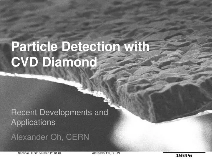
Particle Detection with CVD Diamond. Alexander Oh, CERN. Recent Developments and Applications. Outline. Introduction Material Studies Particle Detector Prototypes Applications in HEP Summary. Sources. RD42 Collaboration University Bonn BaBar, SLAC CMS, CERN.

E N D
Particle Detection with CVD Diamond Alexander Oh, CERN Recent Developments and Applications Alexander Oh, CERN
Outline • Introduction • Material Studies • Particle Detector Prototypes • Applications in HEP • Summary Alexander Oh, CERN
Sources • RD42 Collaboration • University Bonn • BaBar, SLAC • CMS, CERN Alexander Oh, CERN
The RD42 Collaboration: Institutes from HEP, Heavy Ion Physics, Solid State Physics W. Adam1, E. Berdermann2, P. Bergonzo3, W. de Boer21, F. Bogani4, E. Borchi5, A. Brambilla3, M. Bruzzi5, C. Colledani6, J. Conway7, P. D'Angelo8, W. Dabrowski9, P. Delpierre10, W. Dulinski6, J. Doroshenko7, B. van Eijk12, A. Fallou10, P. Fischer20, F. Fizzotti13, C. Furetta8, K.K. Gan14, N. Ghodbane11, E. Grigoriev21, G. Hallewell10, S. Han14, F. Hartjes12, J. Hrubec1, D. Husson6, H. Kagan14;*, J. Kaplon15, R. Kass14, M. Keil20, K.T. Knoepfle16, T. Koeth7, M. Krammer1, A. Logiudice13, R. Lu13, L. Mac Lynne7, C. Manfredotti13, D. Meier15, D. Menichelli5, S. Meuser20, M. Mishina17, L. Moroni8, J. Noomen12, A. Oh15, M. Pernicka1, L. Perera7, R. Potenza22, J.L. Riester6, S. Roe15, A. Rudge15, S. Sala8, M. Sampietro18, S. Schnetzer7, S. Sciortino5, H. Stelzer2, R. Stone7, C. Sutera22, W. Trischuk19, D. Tromson3, C. Tuve22, B. Vincenzo22, P. Weilhammer15, N. Wermes20, M. Wetstein7, W. Zeuner11, M. Zoeller14 1 HEPHY, Vienna, Austria 2 GSI, Darmstadt, Germany 3 LETI/DEIN/SPE/CEA Saclay, France 4 LENS, Florence, Italy 5 University of Florence, Italy 6 LEPSI, IN2P3/CNRS-ULP, Strasbourg, France 7 Rutgers University, Piscataway, U.S.A. 8 INFN, Milano, Italy 9 UMM, Cracow, Poland 10 CPPM, Marseille, France 11 II.Inst. f. Exp. Physik, Hamburg, Germany 12 NIKHEF, Amsterdam, Netherlands 13 University of Torino, Italy 14 Ohio State University, Columbus, OH, U.S.A. 15 CERN, Geneva, Switzerland 16 MPI f. Kernphysik, Heidelberg, Germany 17 FNAL, Batavia, IL, U.S.A. 18 Polytechnico Milano, Italy 19 University of Toronto, Canada 20 Universitaet Bonn, Bonn, Germany 21 Universitaet Karlsruhe, Karlsruhe, Germany 22 University of Roma, Italy * Spokespersons Alexander Oh, CERN
Introduction • Historical Overview • 1913 Röntgen, Joffé, x-ray detection • Resistivity changes of different materials under x-rays exposure • 1941 Stetten, Counter experiments with natural diamond • Alpha particle detection with natural diamond • 1945 van Heerden, Crystal Counters • Wide range of crystal counters investigated, also diamond. • 1984 Angus & Hayman • Low pressure, metastable growth of diamond and diamond-like phases • 1994 Tesarek et al. • Performance of a Diamond Tungsten Calorimeter • “First thermo-luminescence experiment”: Robert Boyle, 28th Oct 1663, Royal Society, London: “I also brought it to some kind of glimmering light by taking it into bed with me, and holding it a good while upon a warm part of my naked body” Alexander Oh, CERN
Introduction • Motivation • LHC and SLHC radiation levels at inner tracking layers O(1015 n cm-2) • Detectors close to IP or at low rapidity • Vertexdetector • Beam monitoring • Some advantageous properties of Diamond compared to Silicon : Alexander Oh, CERN
Introduction: Diamond properties Property______________________Diamond_____________Silicon band gap 5.47 1.12 mass density [g/cm3] 3.5 2.33 dielectric constant 5.7 11.9 resistivity [Wcm] >1011 2.3e5 breakdown [kV/cm] 1e3...20e3 300 e mobility [cm2/Vs] 2150 1350 h mobility [cm2/Vs] 1700 480 therm. conductivity [W / cm K] 10..20 1.5 radiation length [cm] 12 9.4 Energy to create an eh-pair [eV] 13 3.6 ionisation density MIP [eh/mm] 36 89 ion. dens. of a MIP [eh/ 0.1 ‰ X0] 450 840 • Low e -> low capacitance • Low Ileak -> low noise • Room temperature operation • Fast signal collection time • MIP signal 1.9 smaller for same X0 • Collection efficiency < 100% Alexander Oh, CERN
Introduction • Diamond material • Synthetic diamond • Chemical Vapor Deposition • Polycrystalline films • New: large homo-epitaxic mono-crystalline films Alexander Oh, CERN
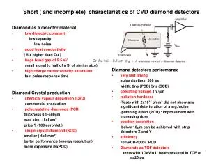
Introduction: CVD process • CVD: Chemical Vapor Deposition • Allows deposition of diamond on large areas in arbitrary geometries. • CVD Diamond is composed of columnar microcrystals. • Growth speed» mm / h Alexander Oh, CERN
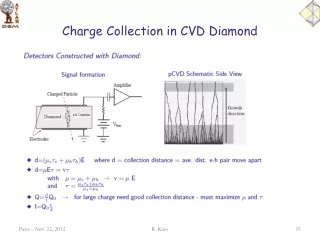
Growth-Side e R h Substrate-Side Introduction • Principle of detector operation collected charge t d “collection distance” e= Q / Q0 collection efficiency Alexander Oh, CERN
Introduction: Trapping • The charge collection efficiency e is for CVDD <100%. • Free charge carriers are captured at defects in the lattice. conduction band valence band Alexander Oh, CERN
Creation of space charge and partial compensation of the external field Charge signal decreases Passivation of traps by occupation with charge carriers. Decrease of active trap concentration and thus increase of charge carrier lifetime. Charge signal increases Introduction: Trapping • Trapping has two consequences: • Polarisation • “Priming” • In polychristalline material the defect concentration is very heterogenous ! Impact on charge signal ! Alexander Oh, CERN
Material Studies Alexander Oh, CERN
Structure 300 mm • Scanning Electron Microscopy (SEM) Pictures show a polycrystalline structure with columnar growth. • A resolved measurement of Bragg reflexes of single crystallites confirms the growth morphology.. • Secondary Ion Mass Spectroscopy allows to analyze the element concentration as a function of position. A increased concentration of foreign atoms at grain boundaries is found. H N O Alexander Oh, CERN
Characterisation with ionising radiation Holes Electrons MIPS, e-(>1,2 MeV), g(10 keV) • constant ionization density • measurement of < e >Z (x) • Weak polarization p (2 MeV), a(5,8 MeV) • Bragg ionization density • measurement of e(z=S,x) • strong polarization X • Resolved measurement can be achieved through beam steering or track reconstruction. Z Alexander Oh, CERN
Characterisation with ionising radiation Si-detector Diamond Beta particle Sr90 source Amplifier Digital Scope • Characterisation with 90Sr-source, Eb,max = 2.28 MeV • Electrons are minimum ionising above 1.2 MeV • ionisation density r=36 eh/mm Alexander Oh, CERN
Material Studies • Signal vs applied Field: • Saturation above 1 V/mm. • Shape governed by m(E) dependence. • Metallization typicallyCr/AuTi/AuTi/Pt/AuTi/W (new) Alexander Oh, CERN
Material Studies • Priming / Pumping • Increase of signal during radiation • Filling of traps increases free carrier lifetime • Empirical fit function: • allows to extract priming fluence F0 • Typical increase factor ~1.5 - 1.8 Alexander Oh, CERN
Material Studies • Polarization • Good contacts are critical • Strong Polarization (probably due to contacts) also observed with MIPS Luis Fernandez Hernando Christoph Ilgner Alick Macpherson Alexander Oh Terry Pritchard Bob Stone Steve Worm Alexander Oh, CERN
Material Studies • Polarization • Observed with mono-chromatic alpha particles alpha particle, E=5.7 MeV, S=14 mm Alexander Oh, CERN
bunchclock beam current Digital Scope HV Material Studies • Synchrotron-radiation HASYLAB • 10 keV photons, l=1600 mm • Beam diameter 50mm .. 100mm • Spatially resolved measurement variable aperture y x Diamond Ti-Pt-Au 10 keV photons Amplifier Alexander Oh, CERN
Material Studies • Polycrystalline structure has impacts on charge collection: Frequency Signal Height [au] Alexander Oh, CERN
Material Studies • The 2D representation shows strong variations and clusters. • The dimensions of clusters are similar to typical grain sizes. • A comparison of back and front side measurement shows similar structures. 1 pixel=50 mm x 50 mm 1 pixel=50 mm x 50 mm Alexander Oh, CERN
Leitungsband Conduction band Valenzband Valence band Material Studies • The photon beam deposits roughly 0.5 pC /mm2 / ms. • The amount of trapped charge can be measured with the TSC (Thermally Stimulated Current) method. • The analysis of the TSC spectrum gives the energy level and concentration of traps. Principle • Occupation of traps through ionisation • Heating of the sample and measurement of I(T) • Subtraction of dark current Alexander Oh, CERN
Material Studies • The photon beam profile defines the volume • After exposure the sample is heated to 300C • The I(T) is recorded • The sample is cooled • The sample is driven to the next scan point • Irradiation for 30s • Heating time to reach 290C is approx. 30s • Cooling time with LN2 to 0C takes approx. 20s • => cycle time 1.5 min ! Alexander Oh, CERN
Material Studies • The results of a scan on 1330 x 1050 mm with a step size of 70 mm. • Also the TSC measurement shows strong non-uniformities ! • Signal scales sub-linear with irradiation time. • The trap concentration and the CCE should be antiproportional • Find correlation of TSC Signal and CCE ! Alexander Oh, CERN
Material Studies • First measurement of CCE and the TSC Signal on the same area • Unfortunately the signal-to-noise is not sufficient to draw a final conclusion….wait for next beam time. Alexander Oh, CERN
Material Studies • Growth Side of a recent polycrystalline CVD diamond Courtesy of Element Six 200mm Alexander Oh, CERN
Material Studies • Non Uniformities qualitatively reproduced by modeling Alexander Oh, CERN
Material Studies • The carrier drift process is simulated for single carriers (electrons and holes) accordingly to the lifetime distribution. • Recombination and trapping is distinguished. • The electric field due to trapped charge is calculated. • The drift path for each carrier is determined by the local electric field and thermal diffusion with 1mm resolution. trapped electrons polarisation field trapped holes • Recombination and trapping is distinguished, priming effect can be modelled…. Alexander Oh, CERN
Material Studies • Comparison of track residuals in the model with and without grain structure • Model with grain structure can qualitatively reproduce residuals observed with diamond pixel detectors. Tommaso Lari (INFN) Alexander Oh (CERN) Norbert Wermes (University Bonn) Alexander Oh, CERN
Material Studies • In 2000 RD42 launched a research program with Element Six to improve the charge collection properties for pCVD diamond. • Impressive improvements achieved beyond the goal set by RD42. Alexander Oh, CERN
Material Studies • Latest Material measured with 90Sr Source: Research Program was successful ! Alexander Oh, CERN
Material Studies • Thinning Experiment • successive thinning of sample and remeasuring collection distance • Gain knowledge on collection properties during growth process Alexander Oh, CERN
Material Studies • Large Wafer Production (5”) possible Alexander Oh, CERN
Material Studies • Radiation Hardness • studied with Protons and Pions on pCVD Strip Detectors • Fluences of 2-3 1015 particles/cm2 • Generally decrease of leakage current with dose observed. • Resolution of Strip detectors increase with Fluence. • Pions damage more than protons. • 50% loss of S/N at 2.9 x 10¹⁵ pions/cm2. • No loss seen for EM radiation up to 10MGy.(Behnke et al., Nucl.Instrum.Meth. A489 (2002) 230-240.) Alexander Oh, CERN
Material Studies • Proton Irradiation 15% loss of S/N 35% improvement in resolution Alexander Oh, CERN
Material Studies • Pion Irradiation 52% loss of S/N 23% improvement in resolution Alexander Oh, CERN
Material Studies • Weaknesses of polycrystalline CVD diamond: • Many grain boundaries -> defects • Non-uniformity of collection properties • Mono-crystalline CVD diamond is a solution: • No grain boundaries -> less defects • Uniform collection properties • First samples available! Alexander Oh, CERN
Material Studies • Mono-crystalline CVD • Perfectly separated from 0e • Narrow Landau distribution • Average 15,000 e Alexander Oh, CERN
Saturation already at 0.2 V/mm • Collection Distance equals Thickness • ~100% efficient Material Studies • Mono-crystalline CVD Diamond Sample CD71415b Diamond Sample CD135 diamonds have been synthesized by Element Six at Ascot Alexander Oh, CERN
Material Studies • Mono-crystalline CVD • No significant priming observed • Trap concentration low Diamond Sample CD135 diamonds have been synthesized by Element Six at Ascot Alexander Oh, CERN
Particle Detector Prototypes Alexander Oh, CERN
Particle Detector Prototypes • Dot detectors • Characterization • Strip detectors • Tracking • Slow VA2 and fast LHC electronics • Pixel detectors • Tracking • CMS and Atlas patterns / electronics Alexander Oh, CERN
Strip Detectors Alexander Oh, CERN
CERN test-beam Setup for Diamond Telescope Alexander Oh, CERN
Two planes of the Diamond Telescope Alexander Oh, CERN
Uniformity in Charge Collection of CVD Diamonds • Measured with MIPS • Similar patterns observed as with photon beam measurement Alexander Oh, CERN
Next Step: • Biased intermediate strips to benefit from charge sharing. • Should improve resolution. Alexander Oh, CERN