Download

1 / 38
380 likes | 495 Views
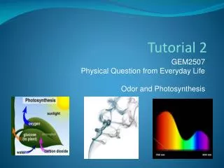
Tutorial 2. Derek Wright Wednesday, January 26 th , 2005. Some Important Units. 10 Å = 1 nm Ex) Si-Si bonds are 2.33 Å, or 0.233 nm 1 micron = 1 m 1 atm = Standard Atmospheric Pressure = 101.3 kPa = 760 torr = ~ 1 bar (1 bar = 100 kPa). Why are we learning about thin film process?.

E N D
Tutorial 2 Derek Wright Wednesday, January 26th, 2005
Some Important Units • 10 Å = 1 nm • Ex) Si-Si bonds are 2.33 Å, or 0.233 nm • 1 micron = 1 m • 1 atm = Standard Atmospheric Pressure = 101.3 kPa = 760 torr = ~ 1 bar (1 bar = 100 kPa)
Why are we learning about thin film process? • It is easier to grow nanometer-scale films vertically than to mask nanometer-scale patterns horizontally. • Combining thin films with very good lithography leads to nanometer-scale devices
Building Devices Exposure/ Developing Deposition/ Growth or Etching Photoresist Application Photoresist Etching
Overview • Deposition (Growth) • Good vs. Bad Films • Physical Methods • Evaporation • Pulsed Laser Deposition • Sputtering • Chemical Methods • CVD • PECVD • Optical CVD • Chemical Solution Deposition • LB Films
So What’s “Good Quality Film”? • A bad film has defects • Defects are different for crystalline and amorphous films • Crystal Defects: • Vacancies (voids), Interstitials (stuff jammed into the lattice), and Dislocations (fractures in the lattice) • Amorphous Defects: • Coordination Defects (dangling bonds)
Deposition: Physical Methods • Physical deposition means that nm sized chunks of material fly at the substrate and stick onto it • The hotter the substrate, the more easily these pieces of material can move around (surface mobility) • They find their point of lowest energy resulting in a better film
Evaporation • Material to be deposited is heated until it becomes vapor phase • The heated material flies into the substrate • The hotter the substrate, the better the film quality • Can deposit very fast relative to other methods, but not always good quality film (up to 200 nm/s film growth)
Pulsed Laser Deposition • Similar to Evaporation method, except uses a laser to heat the material to be deposited • Different because the intense energy creates a plasma • Plasmas not only contain inert material, but also ions and radicals which could chemically react with the surface • Depends on chemistry of reactants
Sputtering • The target (material to be deposited) and substrate are placed facing each other • A plasma is ignited between them under vacuum • A voltage bias between them causes ions from the plasma to ram into the target • The ions eject pieces of the target that “sputter” onto the substrate
Magnetron Sputtering • A big magnet is used to force the electrons into spiral paths so that they spend more time ionizing neutral gas particles • This increases the number of ions • More ions increases the chances of knocking out some of the material to be sputtered • Increases efficiency
Deposition: Chemical Methods • In chemical deposition, the material being deposited on the substrate reacts with the surface • Form bonds with the surface • Chemical reaction with the surface • The substrate as well as reactant temperature play a role in the rate of reaction
Chemical Vapor Deposition • Precursor gas (a gas phase version of what will be deposited on the surface) is pumped into the reaction chamber • It’s heated until reactive species form • Ex) SiH4 SiH2 + H2 • The reactive species chemically interact with the surface to stick to (or react with) it • Surface properties and temperature can determine how well something sticks
Plasma Enhanced CVD • Uses an RF or microwave E-field to strip electrons off the precursor gasses • Since e- are so much lighter than the rest of the molecule (ion), they accelerate in the E-field faster than the molecules
Plasma Enhanced CVD • By the time the E-field changes direction (at RF or microwave frequencies) the electron has gained a lot of momentum and the remaining molecule (ion) has barely started to move • Thus, the e- have a high temperature and the molecules (ions) have a low temperature • This means that the substrate can have a lower temperature, too • Enables new substrates like glass and plastic • This is how TFT-LCD displays can be made
Electrode RF Source Plasma Gas Substrate Plasma Enhanced CVD
Optical CVD • Not always applicable • Uses different wavelengths of light to break precursor gas bond to form reactive species • Ex) Cl2 + h (photon) 2Cl (radicals) • Also enables low temperature deposition
Chemical Solution Deposition • Material is deposited on the substrate in the liquid state • Spin Coating: Some liquid is placed on the substrate and it’s spun really fast until only a thin coating is left • Dip Coating: Dunk the substrate in solution • Spray Coating: Like spray painting the substrate • Screen Printing: Put a stencil on the substrate and use a squeegee to pull solution across • Ink-jet Printing: Same as in an ink-jet printer for a PC
Langmuir-Blodgett (LB) Films • A form of dip coating • You have a solution with a layer of special molecules on the surface • One side of the molecule is water-soluble, and the other is not (like soap) • Thus all the molecules are aligned on top of the solution
Langmuir-Blodgett (LB) Films • When you dunk the substrate in, you get a monolayer (one layer) of aligned molecules on the substrate • If you keep dunking it you’ll get a new layer each time • The water soluble side of one layer aligns with the water soluble side of the next (alternating alignment)
Building Devices Exposure/ Developing Deposition/ Growth or Etching Photoresist Application Photoresist Etching
Lithography • When a pattern is applied to the substrate • The most common is optical lithography where a mask is used to expose a pattern onto a substrate • Like how a transparency on an overhead projector works • The better the lithography, the smaller the feature size • Small feature size nanoelectronics
Optical Lithography • “Resist” is spin-coated onto the substrate • A “mask” is placed in front of the substrate • A mask is a clear plate with a pattern on it, like an overhead transparency • A light shines through the uncovered parts of the mask and chemically changes the resist (exposure) • The exposed resist is etched away with a solvent (developing)
Optical Lithography • Smaller features need smaller wavelengths of light • UV: 365nm - 436nm • Deep UV (DUV): 157nm - 250nm • Extreme UV (EUV): 11nm - 14nm • X-ray: < 10nm
Optical Lithography • Three types: • Contact: The mask is directly against the substrate – good minimum feature size, bad for the mask and substrate to touch • Proximity: The mask is a few m away from the substrate – degrades minimum feature size but good for reliability because mask doesn’t touch substrate • Projection: Lenses are used to focus the mask’s image onto the substrate – good minimum feature size, good for reliability
Extreme UV Lithography • Pretty soon UV lithography will hit the limit in terms of minimum feature size • EUV is the next step • Few materials allow EUV light to pass through, so reflective (instead of transmissive) optics must be used • Mask pattern must be really absorbent to EUV light, so heavy metals are used
X-ray Lithography • After EUV comes X-ray lithography • Enables super-high resolution pattern transfer • There are technical hurdles to overcome before x-ray lithography systems are in place • Synchrotrons need to be further developed as a source for x-rays
E-beam Lithography • Uses a focused beam of electrons to directly write to the substrate • Works much like a CRT TV – an electron gun fires electrons and the beam is directed with magnetic fields • There is a limit to how many electrons can be in the beam because they will start to repel each other and blur the beam
E-beam Lithography • Very precise, but very slow method • Can be accomplished in two ways: • Use a narrow beam and turn it on and off to write or not write a pixel • Use a wide beam and a mask to block the parts that shouldn’t be written • Typically very slow and costly – good for making optical lithographic masks for use in UV, EUV, and X-ray
Nano-imprint Technology • Much like forging steel, except at a very small scale • A stamp is fabricated at the nm-scale using traditional process methods • A substrate is coated with some kind of polymer • The polymer is stamped with the nm-scale stamp • The polymer is either cured with heat or light
Thank You! • This presentation will be available on the web.