Download
1 / 21
260 likes | 891 Views
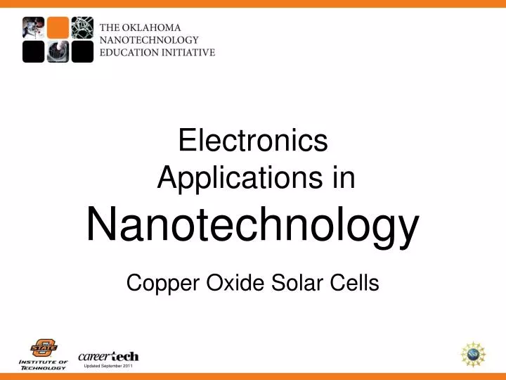
Electronics Applications in Nanotechnology. Copper Oxide Solar Cells. Image by HighPoint Learning. Image by HighPoint Learning. Image by HighPoint Learning. Image by HighPoint Learning. Image by HighPoint Learning. Image by HighPoint Learning. Image by HighPoint Learning.

E N D
Electronics Applications in Nanotechnology Copper Oxide Solar Cells
Calculate and record the Power Power(Watts) = Voltage(Volts) x Current(Amps) Measure the Surface Area of the copper oxide Area(meter2) = Length(meter) x Width(meter)
Power of solar cell =______________ W Surface Area of the copper oxide = ______m2 Sun’s Energy = 1000 W/m2 Calculate the Efficiency of the cell %Efficiency = Power(watts) Sun’s Energy(Watts/meter2) x Surface Area(meter2) Efficiency = _______________%
Compare the Surface Areas of these cells Images by HighPoint Learning r =1.25 h=1.5 3 3 3 3 A= length x width + 2πrh = 20.78 A= length x width = 9
Although the Efficiency should stay the same, increasing the Surface Area is a valid strategy to make an inefficient cell usable. Image by HighPoint Learning r =.125 h=1.5 3 3 A= length x width + 2πrh x64 = 84.4
%Efficiency = Power(watts) ÷Sun’s Energy(Watts/meter2)x Surface Area(meter2) Image by HighPoint Learning 0.9W 2.078W 8.44W
Dye Sensitized Solar Cells cc by Ronald Sastrawan cc by M.R. Jones
How is nanotechnology being used in solar applications? What are some of the new materials in solar cells? What are some new strategies being used in solar cells?
This module is one of a series designed to introduce faculty and high school students to the basic concepts of nanotechnology. Each module includes a PowerPoint presentation, discussion questions, and hands-on activities, when applicable.The series was funded in part by:The National Science FoundationGrant DUE-0702976and the Oklahoma Nanotechnology Education InitiativeAny opinions, findings and conclusions or recommendations expressed in the material are those of the author and do not necessarily reflect the views of the National Science Foundation or the Oklahoma Nanotechnology Education Initiative.
Image CreditsJones, M.R. (Designer). Dye Sensitized Solar Cell Scheme.png [Digital Diagram]. Wikimedia Commons (commons.wikimedia.org)Molhave, Kristian (Professor) and Martinsson, Thomas (Designer), Epitaxial Nanowire Heterostructures SEM image.jpg [Scanning Electron Microscope image], United Kingdom, Wikimedia Commons (commons.wikimedia.org) National Renewable Energy Laboratory (Designer). Carbon Nanotubes.jpg [Digital Image]. United States. Wikimedia Commons (commons.wikimedia.org)Sastrawan, Ronald. (Designer). Dye.sensitized.solar.cells.jpg [Digital Image]. Wikimedia Commons (commons.wikimedia.org)
ReferencesBerger, Michael. (2010). Improved design for dye-sensitized solar cells includes quantum dot antennas. NanoWerk. Retrieved from http://www.nanowerk.com/spotlight/spotid=15000.phpGrätzel, Michael. (2003). Dye-sensitized solar cells. Journal of Photochemistry and Photobiology C: Photochemistry Reviews. Issue 4. Pages 145–153.Williams, Linda and Dr. Wade Adams. (2007). Nanotechnology Demystified. [Kindle Version] doi: 10.1036/0071460233Wilson, Michael, Kanangara, Kamali, Smith, Geoff, Simmons, Michelle, & Raguse, Burkhard. (2004). Nanotechnology: Basic Science and Emerging Technologies. [Kindle Edition] Retrieved from http://www.amazon.com