Download
1 / 3
30 likes | 191 Views
VerilogA Overview. The schematic of the VerilogA transistor model is shown here. It is a table lookup-based model. The tables for I d V g , C gd and C gs are obtained using the TCAD models

E N D
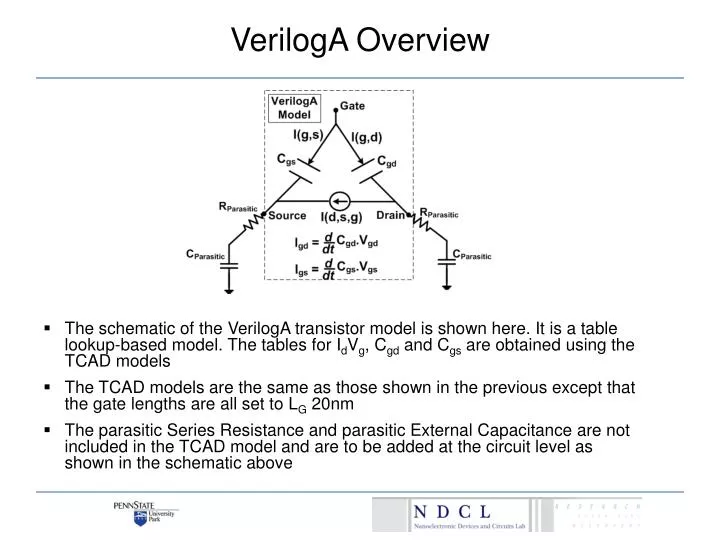
VerilogA Overview • The schematic of the VerilogA transistor model is shown here. It is a table lookup-based model. The tables for IdVg, Cgd and Cgs are obtained using the TCAD models • The TCAD models are the same as those shown in the previous except that the gate lengths are all set to LG 20nm • The parasitic Series Resistance and parasitic External Capacitance are not included in the TCAD model and are to be added at the circuit level as shown in the schematic above
Assumption for TFET VerilogA Models • For the Tunnel FETs, we assume identical drive-currents for the n-channel and p-channel transistors • The electron and hole Density-of-States can be quite different in III-Vs. We assume different Gate capacitances for the n-type and p-type transistors • For Si MOSFETs, we assume identical drive-currents and gate capacitances for n-type and p-type transistors
Spectre Circuit Simulation • In order to execute the circuit simulations you need to have Virtuoso Spectre Circuit Simulatorinstalled • In order to run the idvg simulation use: spectre InAs_ntfet_idvg.scs • In order to run the FO1 inverter simulation use: • spectremdl –b inverter_InAs_tfet_FO1.mdl –d inverter_InAs_tfet_FO1.scs –measure inverter_InAs_tfet_FO1.measure • In order to run the Ring Oscillator simulation use • spectremdl -b InAs_Ring_Oscillator.mdl -d InAs_Ring_Oscillator.scs –measure InAs_Ring_Oscillator.measure