Download
1 / 7
70 likes | 205 Views
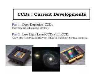
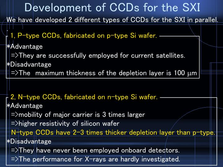
Development of CCDs for the SXI. We have developed 2 different types of CCDs for the SXI in parallel. . *Advantage =>They are successfully employed for current satellites. *Disadvantage =>The maximum thickness of the depletion layer is 100 m m.

E N D
Development of CCDs for the SXI We have developed 2 different types of CCDs for the SXI in parallel. . *Advantage =>They are successfully employed for current satellites. *Disadvantage =>Themaximum thickness of the depletion layer is 100 mm 1, P-type CCDs, fabricated on p-type Si wafer. 2, N-type CCDs, fabricated on n-type Si wafer. *Advantage =>mobility of major carrier is 3 times larger =>higher resistivity of silicon wafer N-type CCDs have 2-3 times thicker depletion layer than p-type. *Disadvantage =>They have never been employed onboard detectors. =>The performance for X-rays are hardly investigated.
Background of developing CCDs with thick depletion layer * L. Strüder et al. developed pn-CCDs with 300 mm thickness of the depletion layer, and it had already employed for XMM-Newton * Steven Holland et al. fabricated MOS CCDs with high resistivity n-type Si wafer and successfully obtained a 300 mm thick depletion layer. Development of the n-type MOS CCDs is under way with a collaboration of Osaka U., Kyoto U., NAOJ (National Astronomical Observatory of Japan) and HPK (Hamamatsu Photonics K.K.).
4.8 mm Specification of test device Specification (design value) Pixel size 14.5 mm x 15 mm Format 328 x 320 Wafer thickness 200 mm Depletion layer 200 mm Illuminated method FI (Front illuminated) Schematic of cross section Depletion layer : 200 mm electrode Fully depleted CCD
Mn ka 5.9 keV Mn kb 6.5 keV counts escape X-ray events Pulse height [ADU] Basic performance Operation temp -70oC Readout speed 60 kHz Spectrum of 55Fe X-ray image 1 pixel size is 14.5 x 15 um n-type CCD Energy resolution 143 ± 3 eV Readout noise 7 electrons p-type CCD 135 eV 5 electrons Basic performance was comparable to that of p-type CCD
Responsivity for soft X-ray spectrum of oxygen K line We investigated the responsivity for soft X-ray by using Oxygen K line : 527 eV Energy resolution FWHM = 81 ± 1 eV We confirmed that this CCD completely collects the signal charges Because this peak has no low energy tail. Oxygen K line 527 eV counts Pulse height [ADU] This CCD have good responsivities for soft X-ray down to 0.5 keV.
22.4 keV 24.9 keV counts Pulse height [ADU] Thickness of the depletion layer Detection efficiency based on http://www-cxro.lbl.gov/optical_constants/ We measured the thickness of depletion layer from the detection efficiency. Solid line : 172 mm Dotted line : 70 mm Spectrum of 109Cd Detection efficiency Energy [keV] Thickness of the depletion layer 172 ± 13 mm Energy resolution 574 eV at 22.4 keV.
Future plan To improve the efficiency below 0.5 keV, We have developed the BI (Back illuminated) CCDs. We will evaluate the performance of this device. Schematic of cross-section Large imaging area (3 x 6 cm) Photograph of engineering model BI Depletion layer electrode FI