Download
1 / 28
290 likes | 553 Views
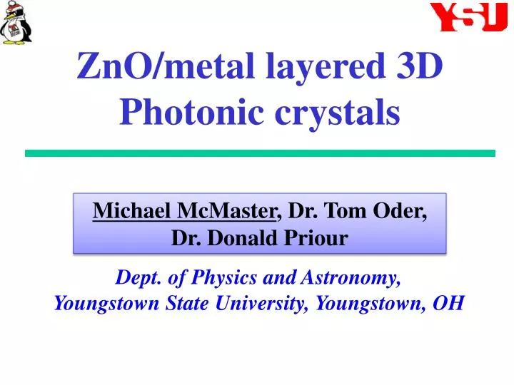
ZnO /metal layered 3D Photonic crystals. Michael McMaster , Dr. Tom Oder, Dr. Donald Priour. Dept. of Physics and Astronomy, Youngstown State University, Youngstown, OH. What to Expect. What is a Photonic Crystal? Experimental Procedure Modeling/Results Conclusion. Photonic Crystal.

E N D
ZnO/metal layered 3D Photonic crystals Michael McMaster, Dr. Tom Oder, Dr. Donald Priour Dept. of Physics and Astronomy, Youngstown State University, Youngstown, OH
What to Expect • What is a Photonic Crystal? • Experimental Procedure • Modeling/Results • Conclusion
Photonic Crystal • “Photonic crystals are materials patterned with a periodicity in dielectric constant, which can create a range of ‘forbidden’ frequencies called a photonic bandgap. Photons with energies lying in the bandgap cannot propagate through the medium. This provides the opportunity to shape and mould the flow of light for photonic information technology.” • J.D. Joannopoulos, Pierre R. Villeneuve & Shanhui Fan • Applications include • Waveguides • LED light extraction • Ultrafast photonic crystal nanocavity laser • High speed communication • High speed information processing
CallophrysGryneus Vinodkumar et. Al. (2010)
Peacock Paridessesostris Weevil and two Longhorns Vinodkumar et. Al. (2010) CERN Courier (2005) Vigneron et. Al. (2012)
ZnO/Cr and ZnO/Al Multilayer Films • Substrate: double-side polished sapphire • Base Pressure: 10-7 mtorr • Preheat temperature:~700°C • Depositions temperature: 300°C • Deposition pressure: 10 mtorr • Ambient gas: Ar • Flow Rate: 10 sccm • Presputter: 3 min • ZnO Buffer Layer: 250 nm • Layer thicknesses: • ZnO/Cr (120 nm/12 nm)x10 • ZnO/Cr (90 nm/ 5nm) x10 • ZnO/Al (170 nm/ 5nm) x8
How can we make 3-D Photonic Crystals? Bottom Up Top Down FIB Holes in 1-D crystals Accurate, small feature size • Shadow mask sputtering • Periodic Array of Pillars • Quick and easy
Some Quick Physics Facts • Index of Refraction: • Snell’s law • The Electric Field Equation:
Mathematical Interlude n1 n2 n3 … nN-1nN ns A0 A1 A2 … … AN As B0 B1 B2 … … BNBs x0 x1 x2 … … xNxs The Electric Field can be shown for different refractive indices as: So we get a vector representing the amplitudes of the wave function. Yeh. (2004)
Mathematical Interlude (continued) We can describe light at the interface of materials with different refractive indices with the dynamical matrices: so that light passing through the interface responds such that . Also, as it travels through a material, the change is shown by the transfer matrix: Yeh. (2004)
Mathematical Interlude (Recap) • By acting on the vector representing light passing through the system with the matrices describing the environment we can predict the transmission spectrum. • Recall: But metals have an imaginary index of refraction (n) so let’s write: But Φhas real an imaginary parts Re(Φ) and Im(Φ) so where we see the Decay term. Yeh. (2004)
1-D Photonic Crystals • Refractive Indices in Visible Spectrum • ZnO 2.0 • Cr 3.2 • Al 1.3 • Layer thicknesses of samples: • ZnO/Cr (120 nm/12 nm)x10 • ZnO/Cr (90 nm/ 5nm) x10 • ZnO/Al (170 nm/ 5nm) x8
Transmission Spectrum Actual Transmission Spectrum Theoretical Transmission Spectrum ?
After Annealing ZnO/Cr 1-D photonic Crystal Theoretical Model
After Annealing ZnO/Cr 1-D photonic Crystal Theoretical Model
Remember those cosines? ZnO/Cr (120nm/12nm)x10 Theoretical Model Photonic Crystal Not a Photonic Crystal
We can Control the Band-Gap! (this Time in Blue) Band-Gap ZnO/Cr 1-D photonic Crystal Theoretical Model
Aluminum • Band-gap is maximized when n1d1=n2d2 • nZnO=2.0 nAl=1.3 • ZnO/Al (170 nm/ 5nm) x8 • We predict a smaller band-gap ZnO/Al 1-D photonic Crystal Theoretical Joannopoulos et. Al. (2008)
EDX Results (Not Chromium Oxide) ZnO/Cr (120 nm/12 nm)x10 Expected Transmission Spectrum if Chromium had oxidized. (CrO3 refractive index 2.55) ZnO/Cr (90 nm/ 5nm) x10 ZnO/Al (170 nm/ 5nm) x8
4-Point Probe Results Bulk Resistivity (Ω∙cm) Pre Annealing Post Annealing ZnO/Cr (120 nm/12 nm)x10 .012 15 ZnO/Cr (90 nm/ 5nm) x10 .0027 310 ZnO/Al (170 nm/ 5nm) x8 too resistive .095
What Next??? • Produce 3-D photonic crystals • using Shadow mask or FIB • Model in higher dimension • TEM/AFM for layer thickness What we Expect What we Hope For • Evidence of 3-D from diffraction pattern • Measureable band-gaps in oblique directions • Improved modeling • both polar and radial angle band-gap dependance • Predict band-gap • Test the effect of electric field on optical the band-gap
References • VinodkumarSaranathan, Chinedum O. Osuji, Simon G. J. Mochrie, HeesoNoh, Suresh Narayanan, Alec Sandy, Eric R. Dufresne, and Richard O. Prum. Structure, function, and self-assembly of single network gyroid (I4132) photonic crystals in butterfly wing scales PNAS 107 (26) 11676-11681 (2010). • Joannopoulos, John D., Steven G. Johnson, Joshua N. Winn, Robert D. Meade. Photonic Crystals Modeling the Flow of Light Second Edition. Princeton University Press (2008). • Yeh,Pochi. Optical Waves In Layered Media: 2nd (second) Edition. Whiley Press (2004). • Peacock feathers prove photonic crystals cast brown light in nature. CERN Courier. Aug 22, 2005 • JoannopoulosJ.D. , Pierre R. Villeneuve and ShanhuiFan. Photonic Crystals: putting a new twist on light. Nature 386 (13) 143-149 (1997) • Vigneron, Jean Pol, and Priscilla Simonis. Natural photonic crystals.Physica B Condensed Matter 407 (20) 4032-4036 (2012)
Acknowledgements • We gratefully acknowledge support of funds from NSF (DMR#1006083) and from the State of Ohio (Third Frontier - RC-SAM). • Support and funds from Youngstown State University • I would also like to thank Dr. Jim Andrews, Jessica Shipman and Matt Kelly and Dr. George Yates for helping with this project.
Any Questions? Xkcd.com