Download
1 / 11
110 likes | 244 Views
Data Acquisition System for NPDGamma. Nadia Fomin April 4 th , 2008 Bon Appetit!. HAZEL/DAQ. VME 1. VME 2. VME 3. You. DAQ!. CLOVER/CONTROL. SSH. SSH. SSH. SSH. 4 rings – 12 Cesium Iodide detectors each. (1 ≤ i ≤ 12) (1 ≤ j ≤ 4). Detector Signal - S j i.

E N D
Data Acquisition System for NPDGamma Nadia Fomin April 4th, 2008 Bon Appetit!
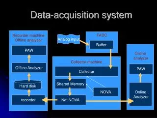
HAZEL/DAQ VME 1 VME 2 VME 3 You DAQ! CLOVER/CONTROL SSH SSH SSH SSH
4 rings – 12 Cesium Iodide detectors each (1 ≤ i ≤ 12) (1 ≤ j ≤ 4) Detector Signal - Sji • Instead of storing the signal from each detector for every neutron pulse: • <Sj>=> Average signal for a ring =4 SUM Signals=>VME3 • Sdiff,ij => Sij -<Sj>=> 48 DIFFERENCE Signals => VME2 • 100 time bins for SUM and DIFFERENCE signals, with each time bin summed over 20 (DIFFs) and 25 (SUMS) samples
4 rings – 12 Cesium Iodide detectors each (1 ≤ i ≤ 12) (1 ≤ j ≤ 4) Detector Signal - Sji • Instead of storing the signal from each detector for every neutron pulse: • <Sj>=> Average signal for a ring =4 SUM Signals=>VME3 • Sdiff,ij => Sij -<Sj>=> 48 DIFFERENCE Signals => VME2 • 100 time bins for SUM and DIFFERENCE signals, with each time bin summed over 20 (DIFFs) and 25 (SUMS) samples
VME 1 VME 2 VME 3 Proton Current Difference Signals Sum Signals RFSF Voltage and Current • => Data from each pulse is written to 3 files, • corresponding to the VME that it came from. • => Data from each pulse is preceded by a header • (in each of the 3 files), including: • Date and time • Time (us) since last pulse (better be 50ms) • Pulse number • DIO data -> most meaningful in VME3, which records the spin sequence • Time since last data write and number of records written Monitor Data (3)
TO 1.1 2.1 3.1 4.1 Fiberoptic Link Receiver TTL N FIFO FIFO TTL NIM Gate/Delay Generator a b delay 1.2 3.2 TTL C TTL Gate/Delay Generator NIM 1.3 3.3 b 1us b TTL N Gate/Delay Generator NIM ?a a gate 1.4 3.4 TTL C gate Gate/Delay Generator NIM Pins 4 Scanclock gate VME 1.3 DIO VME 1.4 Alphi VME 1.? Joerger VME 2 Pins 2 Clock out
T0 Copy to VME2 trigger reset Gate ff 1.1 2.1 3.1 5.1 A B 6.1 4 TTL NIM RESET Gate/Delay Generator 4-fold Logic Gate ttl T0 FIFO Gate/Delay Generator trigger a 1.2 5.2 6.2 b N Gate/Delay Generator b TTL 4-fold Logic Gate NIM reset c TTL c out delay 1.3 2.3 Gate 80 ns 5.3 3.2 b TTL C FIFO A Gate/Delay Generator NIM b B Gate/Delay Generator nim a a 1.4 5.4 TTL TTL N Gate/Delay Generator NIM c Spin Seq Out d c SF out gate d gate Note: Wire on right VME 1.3 DIO VME 1.4 Alphi VME 1.7 Joerger WF GEN VME 1.8 Joerger RFSF T0 8 14 | 17 Scanclock 6 4 T Clock out 2 12 VME 3
b a 1.1 2.1 3.1 4.1 5.1 6.1 10.1 8.1 N TTL NIM COINC FIFO FIFO COINC Gate/Delay Generator b b Gate/Delay Generator Gate/Delay Generator 1.2 2.2 3.2 5.2 6.2 7.2 C TTL FIFO FIFO COINC COINC Gate/Delay Generator NIM b TTL A 8 us a 1.3 a 3.3 5.3 6.3 8.2 4.2 C TTL NIM FIFO FIFO Gate/Delay Generator RFSF T0 Gate/Delay Generator Gate/Delay Generator Gate – 1us a 1.4 a 3.4 5.4 6.4 In - ? N TTL NIM FIFO FIFO Gate/Delay Generator b Gated T0 Out – 10 ns wide b ttl 9.1 1 us - wide Ext. Trig Gate/Delay Generator Digital Delay Pulse Generator a 60Hz Ref b nim Pins 14 9.2 COINC Joerger Scalar VME 1.3 DIO VME 1.5 LeCroy 1182 VME 1.6 LeCroy 1182 10.2 Gate/Delay Generator Arm In T0 1 1 us delay TTL 2 3 Pins 2 VME 1
Current Status: • After some changes, VME1 and VME3 take data (huge improvement from last week when none worked) • VME2 is not completely operational (takes data even when T0 cable is unplugged) • Once it’s up and running, a noise measurement will be done, and then work on the 60hz “upgrade” will seriously begin SNS – 60 Hz operation Doing the naïve software switch, and scaling 20Hz->60Hz, VME2 (largest volume of data) can’t keep up. Issue -> DMA transfer, ADCs can’t read/write simultaneously
Ideas : • Figure out the minimum amt of time that VME2 needs to read out the ADCs, see if that can be found during the SNS pulse. • Problem: All neutrons are slow and probably useful. Upside: If enough time, no money or significant coding/procedural changes. • Add more memory to the ADCs, so that 8 pulses can be stored (one octet), read out every 9th pulse. • Problem: Costs money. Upside: Lose few good pulses. • BUT! SNS pulses are shorter, so 8 might already fit! • 3. Possibly alter the spin sequence, so that every nth (3rd?) sequence is garbage and use that time for data transfer. So, we'd still have an octet, but it would be a subset of 12 spin sequences. Problem: Throw away a third of good pulses. • Example: (1,0,0,1,0,1,1,0)-> (1,0,X,0,1,X,0,1,X,1,0,X) • 4. Installing a real-time kernel. Not sure how that'll fix the problem.