Download
1 / 42
420 likes | 609 Views
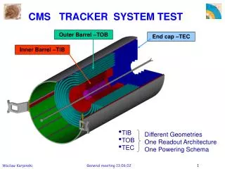
CMS Tracker for the SLHC (A work in progress). Joseph R. Incandela University of California, Santa Barbara 10/10/06. Outline. The SLHC environment Specifications for an SLHC tracker ATLAS straw man tracker for SLHC CMS Workshop conclusions Some general considerations

E N D
CMS Tracker for the SLHC(A work in progress) • Joseph R. Incandela • University of California, Santa Barbara • 10/10/06
Outline • The SLHC environment • Specifications for an SLHC tracker • ATLAS straw man tracker for SLHC • CMS Workshop conclusions • Some general considerations • A variety of possibilities • A variety of possible technologies • A limited amount of money, and how much time? • Cost estimates • A road map for CMS • Some final remarks.
From P.Allport @Hiroshima ‘06 3
SLHC Environment • Tracker designed for 10 y operation at L = 1034 cm-2 s-1 • L = 1035 cm-2 s-1 primarily requires • Finer granularity & greater radiation tolerance. • How short is a strip before it becomes a pixel? • ATLAS: short strips (~3cm). ~ more underlying event (UE) tracks in jets vs. LHC • Alternatively one could consider “Long Pixels” (~1-10 mm) • Reduce UE contribution to jets • 3D track hits • L1 trigger potential
Tracker input to L1 trigger • Will be required • To maintain 100kHz L1 rate & 6.4 µs latency for compatibility with existing systems, and buffer depths • Track trigger • Even partial tracks are useful • Match to ECAL or Muon • Processing on-detector* • Reduce power & latency • But challenging to implement Concepts need details Muon L1 Trigger rate at L= 1034 cm-2.s-1Very limited rejection power without tracker
But...material is not a myth… CMS ATLAS Power reduction and delivery are huge challenges This argues against many pixel layers…
Material budget • Physics performance would benefit from less material • However pixel systems will not reduce power density, currently: • inner microstrips: ~400 W.m-2 Pixels: ~5000 W.m-2 • (intermediate variants likely) • Modern ASIC technologies might use less FE power • But Nchannels will increase, & lower Vsupply increases currents • Power reduction and delivery are huge challenges G. Hall, Imperial College CMS Tracker Meetings, CERN - August 2006
e.g. n-in-p under consideration: Full depletion unnecessary 9
From P.Allport Hiroshima ‘06 10
CMS SLHC Workshop (4th) Perugia, April 2006 • Technology Session • Optical Links, Data transmission, Serial Powering, Mechanics with Rapid Prototyping, Irradiation effects and characterization of 130nm CMOS • New Pixel Layer(s) • Concepts/considerations for new pixel layers, Technologies and materials • Trigger Upgrades • Concepts/designs of triggering layers, Technology developments, TTC upgrade • Full agenda & talks, see • Perugia Workshop
CMS Workshops: Conclusions • Power is a major concern • Despite trend to lower supply voltage in 0.13µm CMOS • Material budget should not increase • Cost must be contained • Pixel systems are not cheaper to build than strips • Large systems are hard to build • R&D and qualification time is always underestimated: • Need: Commonality, Modularity, Automation, Outsourcing. • Sensors must be radiation hard • Mainly an issue for the innermost layers • Off-detector electronics will benefit from technology evolution • Especially digital processing (FPGA’s, FED) and optical links G. Hall, Imperial College
CMS Considerations • What to keep and what to change? • All of the tracker could end up needing to be replaced. • TOB may not sustain fatal radiation doses, but will it function at high efficiency for 2+ decades ? • Capabilities • Tracking/tagging efficiencies/purities to not deteriorate • Track Triggering L1 • The Rub • It must be affordable and buildable in finite time and.. • Material reduction desirable – at least in central region. • The essential conflict: • Fine granularity & trigger (Long) Pixels Mass and Cost Issues • Does ATLAS have the right idea with short strips?
Detector Layout CMS Perugia Workshop Optimise (Low mass? Cheaper?) Could be strips, possibly short, maybe alternate readout? y x Add stacked layer at r~10cm & r~20cm y Detector Dimensions: 120cm(z)x20cm(r) & 60cm(z)x10cm(r) z Pixel Pitch: 10μm(r)x200μm(z)x20μm(φ) J.Jones Imperial College London (Perugia Workshop) 14
Tangent-Point Reconstruction α 15 J.Jones Imperial College London (Perugia Workshop)
Tangent-Point Reconstruction • Assume IP @ r=0 • Angle αdetermines pT of track • Correlation is fairly ‘pure’ provided separation is small and pixel pitch is small. (Improves with radius) • If sensors are precisely aligned, column number for hit pixels in each layer can be compared • Finding high-pT tracks becomes a relatively simple difference analysis α 16 J.Jones Imperial College London (Perugia Workshop)
Difference Analysis in Practice • Nearest-neighbour example 5 - 5 = 0 ≤ ± 1 pass 3-1 = 2 > ±1 fail 1 2 3 4 5 6 7 8 9 1 2 3 4 5 6 7 8 9 8-8 = 0 ≤ ±1 pass y 8-9 = 1 ≤ ±1 pass x J.Jones Imperial College London (Perugia Workshop) 17
Double Stack pT Measurement [e.g. Stacked layers at 10 and 20 cm] • Use centre-point of each pair to measure sagitta • Calculate pT in the usual way… (assuming r=0) • Should give pT up to 100GeV (50% error) • Back of envelope calculation (so far) • Study underway • Gets better at low pT • Can be used for low-pT (1-2GeV) ? • Is this important? From J.Jones Imperial College London (Perugia Workshop) 18
CMS Tracker UpgradePossible High Pt Discrimination SchemeStacks of Sensor Pairs, improved local Pt measurement Straw-man Layout Example 12 Measurement Layers Organized in 3 Super-Layers Each Super-Layer = Stack of 2 Sensor Pairs (4 measurement layers / Super-Layer) Inner Super-Layer ~ 20cm (?) Middle Super-Layer ~ 60cm Outer Super-Layer ~ 100cm Marcello Mannelli Long Pixels For CMS Tracking 19
Sensor Read-out chips Processing chips Bus Signal transport, Control Power CMS Tracker UpgradeChallenges, Technology Questions & Options • Connectivity will be crucial at several levels: • Chip to sensor: low cost bumps?, beyond bumps? MAPS, SOI, … ? • Chips within Sensor Pair (module): bumps to Bus? • Modules with Stack of Sensor Pairs: flex PCB? Bumps ? MAPS, SOI ? Flex PCB? Mechanical support for Stack of Sensor Pairs M. Mannelli et al.
Stacked layers • Many people arrived at similar concept independently… • Advantages: • Online • Trigger: Fast track stub matched to ECAL or Muon system • To limit readout reduce power consumption • Material • Single mechanical support for multiple sense layers • Short pixels powerful pattern recognition fewer layers • But… • Requires something new technical/schedule risks, costs
What’s new? • Technologies discussed in Perugia • Hybrid pixels - now well established but… • Need alternative sensor technology for small radii • Bump-bonding access & cost - particularly for large volumes? • SOI – monolithic pixels • In principle may work – at early stages of development • MAPS - significant expertise in the field • At issue: <100% sensitive, Q collection speed, radiation tolerance • Amorphous-Si on CMOS • At issue: sensor quality, signal quality, process availability • 3D-sensors • At issue: maturity • Short strips for outer layers • At issue: readout: power/cost/material… • Cost an issue in every case.
ionizing particle • Short distance between electrodes: • low full depletion voltage • short collection distance • more radiation tolerant • than planar detectors!! “Standard” 3D detectors - concept Proposed by Parker et al. NIMA395 (1997) p-columns n-columns wafer surface n-type substrate M. Boscardin CMS workshop 4 April 2006 Perugia 23
KEKSOI 24 T. Tsuboyama, Vertex 2006, Perugia Sep. 28, 2006
KEKSOI 25 T. Tsuboyama, Vertex 2006, Perugia Sep. 28, 2006
CMS Tracker UpgradeChallenges, Technology Questions & Options Sensor Radiation Hardness & Sensor to chip connectivity • Integrated Pixel Sensor • Separate processing of sensors and read-out chip => can make radiation hard • Low capacitance of ~ 1mm long pixel => much lower noise than ~ 10cm strips • thin (20~50um) p-on-n is good candidate for radiation hard sensor structure • Relatively low leakage current => simple DC coupling? • Can it work at lower radii, with even smaller pixel size (lower noise)? • Hybrid technology used in present generation of Pixel detectors not suited to very large tracking device ? • Investigate how best to achieve effective connection of read-out chip to sensor with modern packaging/stacking technology Marcello Mannelli Long Pixels For CMS Tracking 26
CMS Tracker UpgradeChallenges, Technology Questions & Options • Integrated Pixel Sensor II • Consider SOI: • The result is • Effectively monolithic structure • Solves Sensor-to-chip connection • Ok for large surfaces, if high yield process • Potential Cons of SOI • Not an Industry Standard substrate • Sensor & CMOS processing coupled • May place constraints on Sensor • May limit choice of Industrial Partners • Time scale: • Prototyping could be started now (Hamamatsu) Marcello Mannelli Long Pixels For CMS Tracking 27
CMS Tracker UpgradeChallenges, Technology Questions & Options • Integrated Pixel Sensor II • Consider SOI: • Discussion ongoing with HPK • Recent meeting in Japan • Thank HPK for ~ 220m2 strip sensors • Continue building on successful collaboration • Goals for a first prototyping run: • Understand basic sensor characteristics • Pixel Pitch: 40 ~ 80 um • Pixel Length: 500um ~ 2mm • Sensor Thickness: 20 ~ 80um • Gain experience with SOI and its constraints • Process sensor before CMOS (will sensor survive CMS process?) • Process sensor after CMOS (read-out vs. sensor geometric constraints?) • Industrial partners and implications on CMOS process Marcello Mannelli Long Pixels For CMS Tracking 28
construction costs • Upgrade cost ~ 200MCHF • Broad brush estimate reported to CMS MB/CB & DG • ~60-70% tracker related • plus staff costs (significant) G. Hall, Imperial College CMS Tracker Meetings, CERN - August 2006
CMS is less symmetric than it seems! Complex, congested routes for services SLHC must fit same volumes Heat load of cables must be removed Cable voltage drops already exceed ASIC supply voltages ASICs have limited tolerance to excursions Tracker services layout G. Hall, Imperial College Experience tells us this will come last even with rigorous systems design approach
Roadmap from previous workshop • Installation of modest system at t = to + 5y may be possible • Lower cost and risk • Allows trial of components or devices, which may still evolve • May be possible to react to LHC conditions • machine, experiment or even discoveries • An evolutionary approach to replacing full tracker? • Ideas are still to gel but must do so soon • CMS proposes common EoI (2006), and LoI (mid-2007) • R&D proposals to be evaluated by CMS, and approved/encouraged G. Hall, Imperial College
You can’t always get what you want… • But how much increase in granularity is actually needed? • Present microstrip occupancies are 0.5% - 2.8% in barrel CMS NOTE 2002/047 G. Hall, Imperial College
High occupancy performance • Heavy Ion collisions simulated • dN/dy ≈ 3000 • occupancies 4 - 30% in µstrips • Results are promising • can use zero suppression • simplest CM algorithms work • ~ 90% for 12 hits • At SLHC expect (at least) • much experience • increased computing power • more powerful FED processing • Some increase in granularity • But how much? • Short strips? C. Roland CMS 2006/031 Reconstruction efficiency/ fake rate Median based CMN offset subtraction with 3 iterations. G. Hall, Imperial College
Minimal Change Approach • Find the minimum granularity increase that’s necessary • Aim to reduce overall power in tracking region (by x2?) • Constrain design by re-using some of “present” structure • eg TOB mechanics is modular, new rods are possible • Is this feasible? To know we need to do our homework: • Track reconstruction studies • Design an S-APV (with digital RO) • Leakage current constraints are more severe: Do we understand them? • New power provision schemes • Explore improved production methods • Baseline designs of foundation components (TTC, optical links) • Even something simple is not so easy to do.
(My) Conclusions • We have concepts and nascent technologies that could eventually yield an outstanding, fine-granularity, and triggerable SLHC tracker • Though services and power dissipation would also need to be squarely addressed. • Timescales now discussed are too short to allow even a minimalist approach without a substantial influx of fresh troops (new collaborators) and money. • The rush to meet an unrealistic schedule could force regrettable decisions • 3 cm short strips ala ATLAS could be the best we can do in such a limited time • But… reducing strip lengths from 10 cm to 3 does not reduce the impact of more underlying event tracks by a factor of 3.3. • The minimalist approach means we accept lower performance standards. • There may be no choice – but it may make sense to make a parallel push for something like stacked long pixels at one or two large radii. • buy back what we are likely otherwise to give up. • All in all this is quite a challenge.
Potential synergy with ATLAS • ATLAS & CMS have exchanged speakers at several workshops • Initial phases of LHC R&D were common • Although many similarities, also important points of divergence • eg sensor design, electrical & optical interfaces, analogue/digital, DAQ design,.. • Possible common efforts • Sharing ASIC processing runs (in CMS & CERN done well for 0.25µm CMOS) • Advantageous to share circuits, evaluate technology and adopt common standards • Share development of common SLHC systems • Optical links and Timing-Trigger-Control system are prominent items • Common effort on power provision - eg DC-DC conversion? • Dialogue with machine • Agree clock speed, verify current systems, information about machine operation • Special tooling • removal and installation of irradiated systems in irradiated environment • Information exchange via regular meetings • Annual LECC workshops are one common forum for electronic R&D • Comparison of cooling system performance might be profitable G. Hall, Imperial College
Conclusions • We will need new collaborators, but the knowledge and experience of those who have built present tracker are essential • Even though heavy commitments remain to complete the present tracker, we need working groups to begin studies • Outline work plan • Definition of new tracker requirements • simulations to establish no of channels, performance • Aim to reduce power budget and unit costs • Define and prototype new pixellated proto-layer with triggering • Define overall structure - reusing present mechanics if possible • External foundations - in LHC-wide collaboration • Standard optical link technology • TTC system capable of use inside tracker • Verify if new methods of power delivery are feasible • Internal foundations • Increase mass production and automation • Further improving cooling performance • Further reducing unnecessary mass G. Hall, Imperial College
Example of a schematic layout • Inner region (~ 4 to ~15 cm) • Super rad-hard “square” pixels • Require new material? • Outer region (~20 to ~120 cm) • Ultra-light Silicon “long” pixels • Of order 100 mm by 1-2 mm • Extremely thin package with both sensor and readout • Order 50-100 mm • Easily cooled and depleted • Super layers: • Pairs with 1-2 mm gap separated from other pairs by 1.5 to 5 cm gaps (depending on radius?) • As few superlayers as possible. C. Hill, JI - UCSB Perugia Workshop Goal: less than 2% Xo per super-layer.
(Current CMS microstrips ~40CHF/cm2 ) R. Horisberger PSI
Cooling costs • Using power has heavy material cost • For present pixel system • Power in ~4% • Power out ~29% • For microstrips • Cables ≈ Cooling • Cables + Cooling + Support ≈ 2x (Sensors+ Electronics)
Noise & granularity • Leakage current shot noise also determines element size • Noise scales ~ (area, time, fluence, shaping time,...)1/2 • How much can be gained by cooling? (ATLAS discuss -35°C) • Ileak will be more significant power burden so must be contained • thermal runaway is increased danger • Is required lifetime again 10 years?