Download
1 / 36
360 likes | 568 Views
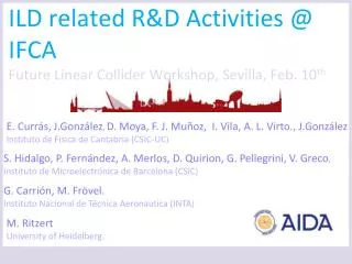
R&D @ IFCA. Jornadas Futuros Aceleradores , Ciemat Dec 2nd ‘09. Iván Vila Álvarez Instituto de Física de Cantabria. R&D at IFCA in a nutshell(1) - Players. Physicists: Celso Martínez, Alberto Ruíz, Marcos Fernández, Amparo L. Virto & Iván Vila. Students: Jordi Duarte, Francisca Muñoz.

E N D
R&D @ IFCA Jornadas Futuros Aceleradores, Ciemat Dec 2nd ‘09 Iván Vila Álvarez Instituto de Física de Cantabria
R&D at IFCA in a nutshell(1) - Players • Physicists: Celso Martínez, Alberto Ruíz, Marcos Fernández, Amparo L. Virto & Iván Vila. • Students: Jordi Duarte, Francisca Muñoz. • Engineer: David Moya (mechanics), Richard Jaramillo (electronics) and J. Gonzalez (software). Jornadas Sobre Futuros Aceleradores , Ciemat Dec 2ndl '09, I. Vila
R&D at IFCA in a Nutshell(2) Technology Network FOS Sensors Double Metal Layer Thin Sensors 5th GICSERV uStrips Sensors Transparent Sensors FOS in Silicon FOS in CFC HPK Sensors CNM Sensors 3th, 4th GICSERV Geometry optimization: Simulation FOS for EMC DCS ALIVABA Jornadas Sobre Futuros Aceleradores , Ciemat Dec 2ndl '09, I. Vila
R&D at IFCA in a Nutshell (&3) - Targets Technology Driven project Jornadas Sobre Futuros Aceleradores , Ciemat Dec 2ndl '09, I. Vila
Outline: R&D lines • R&D on sensors • Improved IR-semitransparent sensors. • Thinned micro-strips sensors with integrated pitch adaptors and embedded FOS. • R&D on mechanics • Integration of Fiber Optic Sensors on Silicon and CF composites • Outlook Jornadas Sobre Futuros Aceleradores , Ciemat Dec 2ndl '09, I. Vila
R&D on Sensors Jornadas Sobre Futuros Aceleradores , Ciemat Dec 2ndl '09, I. Vila
RD on Sensors: IRuS for alignment • Statement of the issue: • Real time position monitoring of the tracker during detector operation with a few microns accuracy. • Reference laser lines going through tracker’s sensors. • Name of the game, increase the IR transmittance of the microstrip sensors introducing minimal modifications to the sensor layout: same materials, avoid fine tuning. • R&D targets: • ILD FTD, SiD tracker, CMS tracker upgrade, AIDA Jornadas Sobre Futuros Aceleradores , Ciemat Dec 2ndl '09, I. Vila
RD on Sensors: IRuS for alignment (2) • 1st Validation of optical simulation software. (done) • 2nd Babysensor baseline design (p on n; AC coupling, 50 um pitch) minimal design modifications to boost sensor IR transmittance. (done) • 3thProduction of IR mini-sensors. (done) • 4th Bench testing of sensors (components ready ) • 5th Sensors irradiation (optical effects) and beam testing (SNR) • 6th Know-how transfer to main vendors. Jornadas Sobre Futuros Aceleradores , Ciemat Dec 2ndl '09, I. Vila
Optical computation validation: Incidence plane Validation of optical simulation software with material samples (planar multilayer samples) Optain optical parameters Validation of optical simulation for layered diffraction grating. Optical simulation of optical test structures and actual sensors. Jornadas Sobre Futuros Aceleradores , Ciemat Dec 2ndl '09, I. Vila
Difference calibrated-fitted thickness= 1 nm !! Difference calibrated-fitted thickness= 2 nm Validation optical simulation: Materials • Simulation predicts calibrated thickness of 6 calibrated bands of SiO2 [d=0-500] nm on a 1-sided polished Si wafer, from Ocean Optics • Si characterized from 1st band (not shown) CEC Meeting, Apr 09 - Marcos Fernandez -IFCA 9 Jornadas Sobre Futuros Aceleradores , Ciemat Dec 2ndl '09, I. Vila
40 diffraction orders 45 nm Al roughness Validation Optical Simulation: diffraction pattern CNM wafer + diffraction Al pattern, using GICSERV07 access. CEC Meeting, Apr 09 - Marcos Fernandez -IFCA 12 Jornadas Sobre Futuros Aceleradores , Ciemat Dec 2ndl '09, I. Vila
%T meas %T sim %R meas %R sim IR transparent mini-sensors Final-Design SiO2 P1 949.9 nm SiO2 FO 1002.7 nm Si / n+ 295 µm SiO2 P1 1003.4 nm OTS1 SiO2 P1 948.0 nm SiO2 GO 49.5 nm P+ / Si / n+ 295 µm SiO2 P1 996.8 nm OTS2 OPTICAL TEST STRUCTURES •Test structures simulated (no fit involved) •n+ and p+ taken optically identical to Si SiO2 P1 929.4 nm SiO2 FO 1002.7 nm Si / n+ 295 µm SiO2 P1 980.5 nm OTS3 OTS4 SiO2 P1 928.4 nm SiO2 FO 1002.7 nm Si / n+ 295 µm SiO2 P1 982.5 nm Jornadas Sobre Futuros Aceleradores , Ciemat Dec 2ndl '09, I. Vila
Sensor measurement vs. calculations. Jornadas Sobre Futuros Aceleradores , Ciemat Dec 2ndl '09, I. Vila
Final outcome projection After last pasivation layer Tmax > 60% (7 layers) Compare with 25% @ CMS Jornadas Sobre Futuros Aceleradores , Ciemat Dec 2ndl '09, I. Vila
Absolute accuracy Determination • Direct comparison with interferometric measurement (accuracy better than 1 um). Sensor to be calibrated Interferometer reflector Wollaston prism Laser Paths Reference granite bench 4th EUDET Annual Meeting, U. Geneve, 20th October '09, I. Vila
Preliminary result with CMS ASPD Sensor • Precision below one micron, accuracy < 1.5 um MICRONS Steps (30 mm) Jornadas Sobre Futuros Aceleradores , Ciemat Dec 2ndl '09, I. Vila
SiTRA Alignment – HPK Alignment sensors. • Two single –sensor modules R/O with APV25 Chips (512ch ) • NIR Transmitance ~ 15-25% “Alignment Hole” 4th EUDET Annual Meeting, U. Geneve, 20th October '09, I. Vila
SiTRA Alignment – SPS Test beam • AIM: • Assessment of SNR for backside removed metallization. • Comparison between track-based and laser alignment. • Testbeam at CERNs SPS • (19. to 26. August 2009) • CERN SPS North Area: H6B • We used the EUDET Beam Telescope to get triggers and tracks • Results • About beam 100Kevents + laser 100Kevents. • Analysis still in progress 4th EUDET Annual Meeting, U. Geneve, 20th October '09, I. Vila
Alignment passage Preliminary TB results • SNR sensor scanning comparing Back side with Al vs. n Back side with Al metallization Particle Beam Scanning points 4th EUDET Annual Meeting, U. Geneve, 20th October '09, I. Vila
R&D on sensors: Thinned ustrips • GICSERV09 access on ustrip thin sensors. • Direct wafer bonding and deep anisotropic etching. • Aim: frame layout design, FEA analysis, mechanical characterization of dummies, bonding tests, bench & test beam testing. Jornadas Sobre Futuros Aceleradores , Ciemat Dec 2ndl '09, I. Vila
Integrated sensor and chip interconnects • Second metal layer for routing and adapting the pitch. • Different geometries are tested. • Run to be launch in January 3th Int. Workshop ,8th October '09, I. Vila
Silicon Optical sensors Reloaded GAPD optical optimization ? Jornadas Sobre Futuros Aceleradores , Ciemat Dec 2ndl '09, I. Vila
R&D on Optical Fiber Sensors Jornadas Sobre Futuros Aceleradores , Ciemat Dec 2ndl '09, I. Vila
R&D on mechanics: Bragg grating • Fiber Bragg Grating optical transducer very common to measure strain and temperature Jornadas Sobre Futuros Aceleradores , Ciemat Dec 2ndl '09, I. Vila
R&D on mechanics: Bragg grating Jornadas Sobre Futuros Aceleradores , Ciemat Dec 2ndl '09, I. Vila
Basic system The number of different Braggs is more than 100; moreover by using an optical switching we can use tents of sensing fiber Optical Spectrum Analyzer Large Bandwidth Light source 1x2 coupler B1 Bn B2 B3 3th Int. Workshop ,8th October '09, I. Vila
OFS & FBG advantages Jornadas Sobre Futuros Aceleradores , Ciemat Dec 2ndl '09, I. Vila
Current R&D activities • (OCT’ 09) MECHANICAL DUMMIES & multi-groove wafer structures. • Exp. validation of FEA simulations. • Conventional KOH anisotropic etching on SOI wafer. 3th Int. Workshop ,8th October '09, I. Vila
Current R&D activities and plans • Preparation of experimental test stand (profilometer + miniclimate chamber and tensile test machine): • Fiber embedding quantitative evaluation. • Validation of FE simulation and extraction of mechanical parameter for thin layers. • Equipment (profilometer) delivered this week. • Thermal test of instrumented dummies to be completed at IFIC 3th Int. Workshop ,8th October '09, I. Vila
OFS work plan – Integration on CF • Integration on CF composite part of CMS R&D • Currently working collaboration agreement with Spanish Aerospace Agency (INTA) for a two year period. • The preliminary plan includes: • Complete the market survey. • Proposal of fiber routing for CMS upgraded tracker • Testing of standalone fibers (irradiation). • CF test structures with bonded or embedded fibers. • Mechanical expansion and compression test under several thermal and humidity conditions. • Experimental validation of OFS vs. electrical expansion gauges. • Comparison with FEA simulations 3th Int. Workshop ,8th October '09, I. Vila
Integrating OFS & carbon fiber composites • For the Track structure would be interesting to use a embedded fiber optic sensor. • more precise and reliable data • It could be use 2 side solution • Better understanding of the results • Useful to quantify the thermal strain Jornadas Sobre Futuros Aceleradores , Ciemat Dec 2ndl '09, I. Vila
What about DEPFETS? • During the thinning process V-groove could be also etched. Integration on other Vertex supporting structures very doable 3th Int. Workshop ,8th October '09, I. Vila
Summary • OFS is a proven technology suitable for building a very fast deformation and temperature monitor • Zero impact on the system material and heat dissipation, and 100% EMC • Other monitoring quantities are in the technology scope: humidity, B field, CO2 • Initial R&D embedding fibers on Silicon. • Preparing R&D on fiber embedding on FC. 3th Int. Workshop ,8th October '09, I. Vila
Plans • R&D Targets: ILD, SiD, SCMS, SBelle • Current activities: • Market survey and contact with OFS vendors • Contacting CF producers (Inta, Fermilab,…) • Next activities: • Testing of standalone OFS. • Prepare CFRP test samples with embedded OPS • Preparing some CF test structures with bonded or embedded fibers. • Mechanical and thermal characterization of the test structures. Jornadas Sobre Futuros Aceleradores , Ciemat Dec 2ndl '09, I. Vila
Short-term Outlook • In 2010: • The IR alignment sensor fully tested with laser and source test bench using ALIVABA electronics. • Irradiation and test beam of IR sensors • Thin, integrated pitch adaptors sensors tested at test bench with APV25 • OFS proof of principle for tracking and pixel structural and environmental monitoring. • Other sensing technologies. Jornadas Sobre Futuros Aceleradores , Ciemat Dec 2ndl '09, I. Vila
GRACIAS Jornadas Sobre Futuros Aceleradores , Ciemat Dec 2ndl '09, I. Vila