Download
1 / 14
140 likes | 155 Views
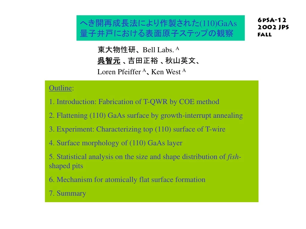
6pSA-12 2002 JPS fall. へき開再成長法により作製された (110)GaAs 量子井戸における表面原子ステップの観察. 東大物性研、 Bell Labs. A 呉智元 、吉田正裕 、秋山英文、 Loren Pfeiffer A 、 Ken West A. Outline : 1. Introduction: Fabrication of T-QWR by COE method 2. Flattening (110) GaAs surface by growth-interrupt annealing

E N D
6pSA-12 2002 JPS fall へき開再成長法により作製された(110)GaAs量子井戸における表面原子ステップの観察 東大物性研、 Bell Labs. A 呉智元 、吉田正裕 、秋山英文、 Loren Pfeiffer A、Ken West A Outline: 1. Introduction: Fabrication of T-QWR by COE method 2. Flattening (110) GaAs surface by growth-interrupt annealing 3. Experiment: Characterizing top (110) surface of T-wire 4. Surface morphology of (110) GaAs layer 5. Statistical analysis on the size and shape distribution of fish-shaped pits 6. Mechanism for atomically flat surface formation 7. Summary
Fabrication of T-shaped QWR by cleaved-edge overgrowth AlGaAs GaAs (110) First MBE growth Second MBE growth in situ cleavage arm 1 GaAs (001) substrate stem (001) Advantages: available to design QW freely at atomic scale. T-wire Rough ARM Flat Disadvantages: MBE growth on (110) * Critical growth condition: surface roughness leading to degradation. STEM
Growth-interrupt annealing treatment Atomically flat surface formation on (110) GaAs layer by growth-interrupt annealing (Jpn.J.Appl.Phys. (2001)) Microscopic PL images and spectroscopy & morphology via AFM of (110) GaAs layer (Appl. Phys. Lett. (2002)) • Application: • The first single wire lasing • (26th ICPS, Edinburgh (2002) 6nm ( 30ML-GaAs) (110) GaAs layer before & after annealing 600 oC 10 min 5 mm X 5 mm 490 oC growth ? Mechanism for flat surface formation:
Characterizing top surface of T-QW : (110) surface 80mm 29.X ML As 3~4 mm 30.0 ML [110] 30.X ML Ga [001] [110]
X 29.26 ML 29.35 ML 29.35 ML 29.55 ML 29.42 ML 29.48 ML At Minus Deviations
P3-06-C 29.58 ML 29.74 ML 29.92 ML 30.09 ML 30.00 ML 30.06 ML 0 and Plus Deviation
P3-06-C 30.15 ML 30.19 ML 30.25 ML 30.25 ML 30.27 ML 30.27 ML At Plus Deviations
Atomic step model and kinetics of surface evolution during annealing
Time evolution of 1-ML-deep pits into atomically flat surface [110] [001] [110]
Summary Characterized: atomically flat (110) GaAs surfaces fabricated by the CEO method with growth-interrupt annealing Statistics of atomic edge stability of 1-ML-deep pits: large fish: round shape ⇔ small fish: thinner shape ! Ga capping three bonds > Ga capping two bonds Proposed: model for atomically flat surface formation. Note: Atomically flat surface consists of Ga capping three bonds
Ga23 01-b 03-c 08-a 13-a 15-b 16-c Sample: 5-18-00.2 (pos. 2)
Ga24 04-d 06-c 01-b 10-c 11-c 09-c Sample: 5-18-00.2 (pos. 3)
Characteristic surface shapes • Spatial distribution of GaAs layer thickness (1 %/mm): • islands & pits on flat surface. • Fish : 1-ML-deep (0.2 nm) • pits at +deviation. • Boat: 2~3-ML-high islands • at -deviation. • Arrowheads: 2-ML-deep pits • at -deviation.