Download
1 / 32
330 likes | 381 Views
Explore the latest developments in superconducting RF cavities for linear accelerators, including electropolishing techniques, baking processes, and high gradient shapes. Learn about the advances in manufacturing techniques and the potential advantages of large grain niobium. Discover the importance of optimizing EP treatment and baking for improved cavity performance.

E N D
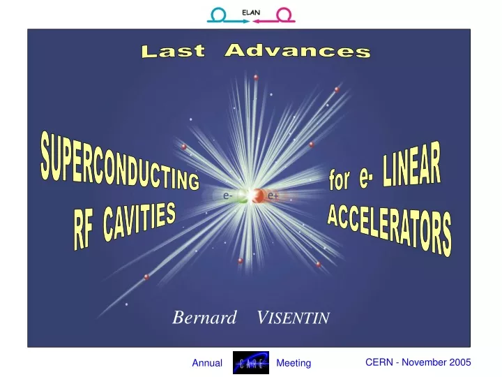
Last Advances SUPERCONDUCTING RF CAVITIES for e- LINEAR ACCELERATORS Bernard VISENTIN
Eventful Year for SRF R&D Single Crystal & Large Grain Cavities Manufacturing multi-cell Cavities ( LL shape) 2005 Eacc Records mono-cell Cavities new shape ( LL & RE ) Fast Baking : experimental show of O role
High Gradients S-LINAC Cost Relative Cost ( €/$/¥ ) C. Adolphsen 1st ILC Workshop Eacc (MV/m) Baseline Configuration Document for ILC (500 GeV) operating @ 31.5 MV/m recommendation Eacc 35 MV/m (including fabrication scatter 5%) 37 MV/m
Recipe for High Gradients Electropolishing + Baking ( EQuench ) ( Q-slope ) B. Visentin - EPAC 1998 K. Saito - SRF Workshop 1997 40 MV/m
where do we stand with ? ELECTROPOLISHING
Electropolishing Oxide attack by HydroFluoric acid : re-oxidation Chemistry : Nb Surface Renewal Electrochemistry Standard Chemistry (BCP) Rotating Anode (+) : Nb cavity Cathode (-) : Al FS ( 1:9 ) V ( 17 volt ) – J ( 60 mA/cm2 ) plateau Nb oxidation : Dunked cavity FNP ( 1:1:2 ) Nb oxidation : Hypothesis: Surface roughness ( better water rinse – lower H field enhancement )
Electropolishing Electropolishing at DESY Faced to this superiority To set up an EP facility for 9-cell cavity L. Lilje - SRF Workshop 2005
Electropolishing Electropolishing at DESY RF tests results on 9-cell cavities TTF Linac 1 GeV 400 MeV 800 MeV 4 MeV 120 MeV ACC6 modulewith 8 EP cavities @ 35 MV/m ( Summer 2006 )
Electropolishing Reproducibility - Field Emission Unfortunately, in spite of the EP success a large spread exists in the cavity production compare to standard chemistry
Electropolishing Optimization of EP Treatment Nb sample mono-cell cavity 9-cell JRA1 - SRF • EP bath impurities • Cathode corrosion (Al) and Sulphur deposition • solution alcohol rinse • EP bath ageing ( Nb dissolved ): HF concentration • F:S concentration 1:9 (9 g/l) 4:9 (23 g/l) • Optimize parameters ( V-I ) • Explore different working zones ( plateau, …) EP test bench for mono-cell F. Eozénou - SRF Workshop 2005
Electropolishing • RMS surface roughness: • fine grain (BCP) : 1274 nm • fine grain (EP) : 251 nm • large grain (BCP) : 27 nm Large Grain Cavity High Gradient shape 1.5 GHz with Standard Chemistry « BCP» Very smooth surface ( EP not necessary ) P. Kneisel PAC 2005 & SRF Workshop 2005
Electropolishing BCP large grain cavity BCP fine grain cavity ( 30 MV/m ) with better surface roughness than EP fine grain cavity @ 40 MV/m Open Question High Gradients @ 40 MV/m are they linked to Electro-Polishing (surface roughness) or just to Electro-Chemistry ? Potential Advantages of Large Grain Nb • Niobium discs sliced directly from ingots • ( saw cut or electrical discharge machining : no forging , no rolling ) • Reduced cost • Less impurities • Quality control more easy adopted as : Alternative Option for ILC 500 GeV WG 5 Report - 2nd ILC Workshop ( Snowmass 2005 )
Electropolishing EP Large Grain Cavities at DESY TESLA Shape (1.3 GHz) – Electropolishing first test (before baking) : Q-slope - 28 MV/m
Where do we stand with ? BAKING
Baking Whatever the niobium structure… ( Single or Poly-crystal,) & Cavity Shape ( HG,LL,RE ) Whatever the fabrication method…( EB Welding or Hydroforming, bulk Nb or clad Nb/Cu) Whatever the thermal treatment… (nothing, 800°C, 1300°C/Ti ) Whatever the chemical treatment… ( Electropolishing or Standard Chemistry ) Baking Wide Application Area in-situ (UHV) T = 110 - 120 °C t = 1 – 2 days TTF 1.3 GHz - Saclay Polycrystalline 1300°C / Ti Chemical Etching 1:1:2 TTF 1.3 GHz - Saclay / KEK Polycrystalline No Thermal Treatment Electropolishing LL 2.2 GHz - JLab Single crystal 800°C – 1250°C / Ti Chemical Etching 1:1:1
Baking Baking Permanent Treatment • T = 120 °C / 2 days • + • Air exposure • for 4 years – • without any particular • precautions • Hydrofluoric Treatment • High Pressure Rinse
Baking Baking Diffusion interstitial oxygen RS Change through electron Mean Free Path ( l ) decrease 110 °C 60 hours in-situ ( UHV )
Baking Explanation of Q-slope Improvement by Baking Doping Effect in Niobium Baking Q-slope Diffusion of Interstitial Oxygen B. Visentin SRF Workshop 2005
Baking Baking Parameters ( T , t ) with Unchanged Oxygen Penetration 2nd Fick's law analytic solutions 110 °C / 60 hours equivalence 145 °C / 3 hours semi infinite solid : C(0,t) = CS thin oxide layer : C(x,0) = Q d(x)
Baking « Fast » Baking ( UHV ) • Infra-Red emitters (short T rise time) • Cavity pumped out ( Ultra High Vacuum ) 145 °C - 3 hours Similarities with Standard Baking
Baking O % from interface Nb2O5 – NbOX / Nb Control oxygen penetration in niobium
Baking Fast Baking : Improvement for Cavity Mass Production Save time & Possibility to simplify the cavity preparation Electropolishing + Ultra Pure Water Rinse Electropolishing + Ultra Pure Water Rinse High Pressure Rinse - 85 bars (FE) High Pressure Rinse - 85 bars (FE) Clean Room ( Class 100 ) Air Baking : T °C /t hours Air Drying : 3 hours Assembly + Helium Test Assembly + Helium Test (RF Test ) RF Test Bed ( Cryostat ) Baking Ultra High Vacuum 110 °C / 2 days 145 °C / 3 hours RF Test RF Test
« Air - Baking » in Clean Room FastAir-Baking on Wet Cavity under LaminarFlow (FE) OK (UHV) Temp. / TimeTurbulences adopted to substitute the “in-situ” baking Alternative Configuration Document ( ILC 500 GeV ) WG 5 Report - 2nd ILC Workshop ( Snowmass 2005 )
Overcome ? 40 MV / m
Nb Cavity Performances ( 1991 - 1999 ) Continuous improvements with Heat Treatments @ 800 and 1400°C, High Pressure Rinse, Baking & ElectroPolishing. 42 MV/m hard barrier ( 2004 )
Quench (SC Breakdown) : thermal effect on local defect if T >Tc (9.2K) or surface peak magnetic field Hp>Hc (2000 Oe) Experimental limitation @ 1750 0e Reduce Hp Ratio Hp/Eacc (determined by geometry) J. Sekutowicz SLAC Talk 2005 K. Saito - SRF 2005 -12% New Shape to Reduce Hp / Eacc TTF : Optimized to reduce field emission & multipacting ( iris rounded – cell rounded far from pill-box geometry) New shape : decrease surface H field increase magnetic volume (for lower P dissipation small Ø iris & maximize R/Q*G parameter) Critical Points : cleaning and preparation (Ep/Eacc increase) - stiffness
Single Cell LL Cavity @ 45 MV/m Single Crystal ( 2.2 GHz ) Standard chemistry P. Kneisel – PAC 2005
courtesy of Kenji Saito Single Cell RE Cavity @ 52 MV/m Fine Grain ( 1.3 GHz ) Electropolishing + Baking R.L. Geng – SRF Workshop 2005
from Kenji Saito Single Cell LL or RE Cavities Eacc > 40 MV/m Obviously new step is crossed with cavity shape modification adopted as : Alternative option for ILC 500 GeV ( Baseline for 1 TeV upgrade ) Eacc > 40 MV/m ( including fabrication scatter ) 42 MV/m WG 5 Report - 2nd ILC Workshop ( Snowmass 2005 )
Multi Cell LL Cavities Four 7-Cell @ 1.5 GHz installed in “Renascence” 3rd prototype CW cryomodule - CEBAF upgrade 12 GeV Vertical tests – Q slope - 25 MV/m C. Reece – SRF Workshop 2005 “ICHIRO” cavities Goal : 51 MV/m T. Saeki – SRF Workshop 2005 Four 9-Cell ( 1.3 GHz )
Conclusions • High gradients required for future e- linear accelerators : • within reach, at least for single cell cavities • Physical explanations ( EP and Baking ) are not well understood : • FundamentalR&D goes on • Main goal : • Technical R&D to optimize and simplify the preparation process • decrease in field emission • better reproducibility of EP ( scatter in performances ) • performing « fast air-baking » in clean room
Acknowledgements • Thank you to my colleagues for providing • information and documents to prepare this presentation • DESY : L. Lilje – J. Sekutowicz • JLab : P. Kneisel – C. Reece • KEK : K. Saito – T. Saeki • Cornell : H. Padamsee – R.L. Geng