Download
1 / 12
120 likes | 276 Views
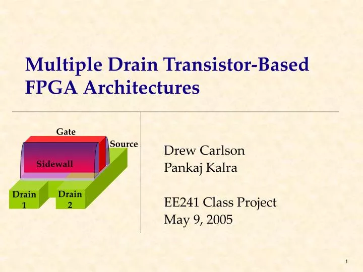
Multiple Drain Transistor-Based FPGA Architectures. Drew Carlson Pankaj Kalra EE241 Class Project May 9, 2005. Si 3 N 4. Q nit. SiO 2. n/n-. n +. P+. D. S. Multiple Drain Transistors. Goal: Reduce cost per fxn Multiplexing + memory in single cell Multiple Drain Transistor [1]

E N D
Multiple Drain Transistor-Based FPGA Architectures Drew Carlson Pankaj Kalra EE241 Class Project May 9, 2005
Si3N4 Qnit SiO2 n/n- n+ P+ D S Multiple Drain Transistors • Goal: Reduce cost per fxn • Multiplexing + memory in single cell • Multiple Drain Transistor [1] • Non-volatile switch connects/disconnects drains from channel • Similar to: Sidewall Flash Memories [2, 3] • Scalable • Reverse-read • Benefits: • Forward write/read • Larger effective widths gate Drain1 D2 S Dn [1] A.Carlson and T.-J. King, Device Research Conf., 2005, to be published. [2] M. Fukuda et al., IEDM Technical Digest, pp.909-912, 2003. [3] Y.K. Lee et al., J. Vac. Sci. & Tech. B, 22, pp.2493-2498, 2004. Carlson / Kalra – MDT-based FPGAs
G D1 S D2 Building a SPICE Model • Subcircuit Model • Driving & coupling MOSFETs • Effective widths from geometry calculations • Resistive LDDs • Process Model • Square law approach • 1-drain MOSFET I-V curves from MEDICI (device sim.) • Fit SPICE parameters to curves Curves: SPICE Markers: MEDICI Vgs = 0.6V, 0.8V, 1.0V. Carlson / Kalra – MDT-based FPGAs
Field Programmable Gate Arrays (FPGAs) • Routing Fabric • Horizontal & vertical channels meet at switch blocks • 70-90% die area • Limiting Constraint: Area • (# switches) x (switch area) • Minimize either / both • Logical Blocks • Program to any function w/ Look Up Table (LUT) LUT D Q > Logic Block 6T Switch [1] H. Schmit and V. Chandra, “Layout Techniques for FPGA Switch Blocks,” IEEE Trans. VLSI Systems, vol. 13, pp.96-105, Jan. 2005. Carlson / Kalra – MDT-based FPGAs
Smaller Switches • Pass Transistor • Up to 7x area reduction • Comparable performance vs. • Buffered Switch • Savings in fanout (pass) vs. SRAM (multiplicity n) (n drains) SRAM SRAM Carlson / Kalra – MDT-based FPGAs
Smaller Switch Blocks • Disjoint • Channel Width = 4, Flexibility = 3, Wpass=10Wmin • 4.37μm x 5.81μm (vs. 124 μm2) • 3 MDT / switch Carlson / Kalra – MDT-based FPGAs
More Routability • Universal • Channel Width = 4, Flexibility = 9, Wpass=10Wmin • 17.73μm x 6.57μm (vs. 394 μm2) Carlson / Kalra – MDT-based FPGAs
S0 S1 S0 SRAM S2 LUT . . S3 SRAM OUT . . . S3 Critical Path . . . . . . . . . OUT SRAM LUT • Total Area 185 Amin • Delay of critical path = 415ps Amin (area of minimum width transistor) = 0.324μm2 (90nm process) Carlson / Kalra – MDT-based FPGAs
S0 S1 0 Precharge 1 1 Output 0 MDT MUX • Pair of double-drain MDTs and pair of pass transistors • 41 MUX 41 MUX • Store configuration bits during programming • Reading 0 • Select MDT drain pulled to low Select Pass tx. • Reading 1 • Precharge signal pulls output to high Carlson / Kalra – MDT-based FPGAs
S1 S0 Precharge S2 S3 . . . . . . . . . OUT MDT LUT • Total Area 87 Amin • Delay of critical path = 370ps 53% area reduction Carlson / Kalra – MDT-based FPGAs
Vpp Vdd Out Programming of MDT • Programming needs not be very fast (done offline) • Store all the configuration bits in a shift register • Tradeoffs • Charge Pumps to get high voltagelevel • MDT Programming • Require high voltage pulse (VG=3V, VD=5V) • Level-shifter circuit to generate high-voltage pulse • Feedback pMOS type • Cross-coupled pMOS type Level Shifter In Carlson / Kalra – MDT-based FPGAs
Summary • Novel device structure studied for reconfigurable applications • MDT based FPGA architecture is proposed • Routing fabric : up to 80% area reduction • LUT: up to 53% area reduction Carlson / Kalra – MDT-based FPGAs