Download
1 / 42
430 likes | 718 Views
Reversible Computing A Requirement for Extreme Supercomputing. Dr. Michael P. Frank, Assistant Professor Dept. of Electrical & Computer Eng. FAMU-FSU College of Engineering ECE Department Graduate Seminar Thursday, September 2, 2004. Abstract.

E N D
Reversible ComputingA Requirement forExtreme Supercomputing Dr. Michael P. Frank, Assistant ProfessorDept. of Electrical & Computer Eng.FAMU-FSU College of Engineering ECE Department Graduate SeminarThursday, September 2, 2004
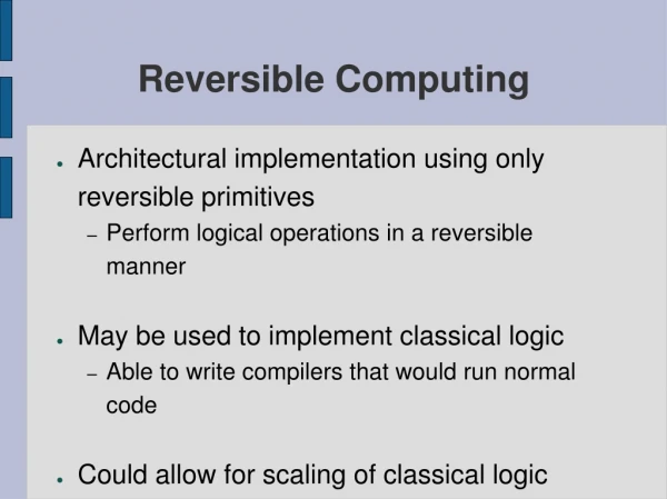
Abstract • The energy dissipated per switching event directly limits any digital system’s performance per unit of power consumption. • E.g., typical logic node switching energy today = ~0.1 fJ. • A 1 MW machine could do “only” 100 PFLOPs. (assuming 105 logic ops/FLOP) • A 1 ZFLOPs machine in today’s tech. would require at least 10 GW! • This is the approximate electrical power consumption of Norway! • Traditional “irreversible” switching mechanisms are subject to a relatively high minimum energy dissipation per signal transition event. • The practical limit for irreversible CMOS may be only ~1 order of magnitude better than today’s technology. • And further, any possible irreversible technology is at best only ~2-4 orders of magnitude better than today’s! • E.g., 1 ZFLOPs, terrestrially at least ~40 MW (non-adiabatic) • Circumventing all these bounds will require moving to increasingly reversible switching mechanisms and logic styles… • With long-term implications for computer architecture, programming languages, and algorithm design… • In this talk, we survey reversible computing principles. • We argue: Reversible computing needs to be more aggressively explored! M. Frank, "Reversible Computing"
Moore’s Law (Devices/IC) Intel µpu’s Early Fairchild ICs M. Frank, "Reversible Computing"
Device Size Scaling Trends Based on ITRS ’97-03 roadmaps (1 µm) Virus Protein molecule Naïve linear extrapolations Effective gate oxide thickness DNA/CNT radius Silicon atom Hydrogen atom M. Frank, "Reversible Computing"
Trend of Min. Transistor Switching Energy Based on ITRS ’97-03 roadmaps fJ Node numbers(nm DRAM hp) Practical limit for CMOS? aJ Naïve linear extrapolation zJ
Important Energy Limits • Near-term leakage-based limit for MOSFETs: • May be ~5 aJ, roughly 10× lower than today. • 10× faster machines, ~4-8 years left on the clock • Reliability-based limit on bit energies: • Roughly 100 kT ≈ 400 zJ, ~100× below now. • 100× faster machines, ~8-15 years to go… • Landauer limit on dissipation per bit erasure: • About 0.7 kT ≈ 3 zJ, ~10,000× below today. • 10,000× faster machines, ~15-30 years left… • No limit is known for reversible computing… • We need to investigate this alternative further. M. Frank, "Reversible Computing"
FET Energy Limit • A practical limit for all transistors based on the field effect principle. • It’s probably not an absolutely unavoidable, fundamental limit. • However, it is probably the biggest barrier to further transistor scaling today. • The limit arises from the following chain of considerations: • We require reduced energy dissipation per logic operation. → Want small ½CV2 logic node energy (normally dissipated when switching) → Want small node capacitance C→small transistor size (also for speed) → Need to lower switching voltage V, due to many factors: • Gate oxide breakdown, punch-through, also helps reduce CV2. → Reduced on-off ratio Ron/off = Ion/Ioff < eVq/kT (at room temperature) • Comes from Boltzmann (or Fermi-Dirac) distrib. of state occupancies near equil. • Independent of materials! (Carbon nanotubes, nanowires, molecules, etc.) → Increased off-state current Ioff and power IoffV, given high-performance Ion. → Also, increased per-area leakage current due to gate oxide tunneling, etc. → Previous two both increase total per-device power consumption floor • Adds to total energy dissipated per logic gate, per clock cycle • Eventually, the extra power dissipation from leakage overwhelms the power/performance reductions that we would gain by reducing CV2! • Beyond this point, further transistor scaling hurts us, rather than helping. • Transistor scaling then halts, for all practical purposes! M. Frank, "Reversible Computing"
Mitigating MOSFET Limits • Reduce the portion of the ½CV2 node energy that gets dissipated • Reversible computing with adiabatic circuits does this • Reduce parasitic capacitances that contribute to logic node’s C • via silicon-on-insulator (SOI) devices, low-κ field dielectric materials, etc. • Use high-κ gate dielectric materials → • Allows gate dielectrics to be thicker for a given capacitance/area • Reduces tunneling leakage current though gate dielectric. Also: • Avoids gate oxide breakdown → allows higher V → indirectly helps reduce off-state conduction. • Use multi-gate structures (FinFET, surround-gate, etc.) to • reduce subthreshold slope s = V/(log Ron/off) to approach theoretical optimum, • s = T/q = (kT/q ln 10)/decade = 60 mV/decade • Use multi-threshold devices & power-management architectures to turn off inactive devices to suppress leakage in unused portions of the chip • The remaining leakage in the active logic is still a big problem, however… • Lower operating temperature to increase Vq/kT and thus IDS on-off ratio? • May also lead to problems with carrier concentration, cooling costs, etc. • Conflicts with the high generalized temperature of high-frequency logic signals • Consider devices using non-field-effect based switching principles: • Y-branch, quantum-dot, spintronic, superconducting, (electro)mechanical, etc. M. Frank, "Reversible Computing"
Reliability-Based Limit • A limit on signal (bit) energy. • Applies to any mechanism for storing a bit whose operation is based on the latching principle, namely: • We have some physical entity whose state (e.g. its location) encodes a bit. • E.g., could be a packet of electrons, or a mechanical rod • If the bit is 1, the entity gets “pushed into” a particular state and held there by a potential energy difference (between there and not-there) of E. • The entity sits in there at thermal equilibrium with its environment. • A potential energy barrier is then raised in between the states, to “latch” the entity into place (if present). • A transistor is turned off, or a mechanical latching mechanism is locked down • The Boltzmann distribution implies that E > T log N = kT ln N, in order for the probability of incorrect storage to be less than 1/N. • For electrons (fermions), we must use the Fermi-Dirac distribution instead… • But this gives virtually identical results for large N. • When erasing a stored bit, typically we would dissipate the energy E. • However, this limit might be avoidable via special level-matching, quasi-adiabatic erasure mechanisms, or non-equilibrium bit storage mechanisms. M. Frank, "Reversible Computing"
Numerical Example • Example: Reliability factor of N=1027 (e.g., 1 error in a 109 gate processor running for ~3 years at 10 GHz) • The entropy associated with the per-op error probability is then:log 1027 = 27 log 10 = 27kB ln 10 ≈ 62 kB = 8.6×10⁻²² J/K • Heat that must be output to a room-T (300 K) environment:kB (300 K) ln 1027 = 2.6×10⁻¹⁹ J (or 260 zJ, or 1.6 eV) • Sounds small, but… • If each gate dumped this energy @ a frequency of 10 GHz, • the total power dissipated by an entire 109-gate processor is 26 W. • Could have at most 4 such processors within a 100 W power budget! • Maximum performance: 4×10²⁰ gate-cyles/sec. • or 4 PFLOPS, if processors require ~100,000 logic ops on average to carry out 1 standard (double-precision) floating-point op • a fairly typical figure for today’s well-optimized floating-point units • Typical COTS microprocessors today have ~100× additional overhead, • Leading to 40 TFLOPS max performance if using these same architectures • A 40-TFLOP supercomputer (e.g. Blue Gene/L) burns ~200 kW today • Only 2,000× above the reliability-based limit! M. Frank, "Reversible Computing"
Von Neumann / Landauer (VNL) bound for bit erasure • The von Neumann-Landauer (VNL) lower bound for energy dissipation from bit erasure: • “Oblivious” erasure/overwriting of a known logical bit moves the information that it previously contained to the environment The information becomes entropy. • Leads to fundamental limit of kT ln 2 for oblivious erasure. • This particular limit could only possibly be avoidable through reversible computing. • Reversible computing “de-computes” unwanted bits, rather than obliviously erasing them! • This enables the signal energy to be preserved for later re-use, rather than dissipated. M. Frank, "Reversible Computing"
s0 t0 0 0 Rolf Landauer’s principle (IBM Research, 1961): The minimum energy cost of oblivious bit erasure Before bit erasure: After bit erasure: (A relatedprinciple wassuggested by John vonNeumannin 1949) Knownto be inone ofthese Npossibledistinctstates … … … Knownto be inone ofthese 2Npossibledistinctstates sN−1 tN−1 0 0 Unitary(one-to-one)evolution - or - Knownto be inone ofthese Npossibledistinctstates s′0 tN 1 0 … … … … s′N−1 t2N−1 1 0 Increase in entropy: ∆S = log 2 = k ln 2. Energy dissipated to heat: T∆S = kT ln 2 M. Frank, "Reversible Computing"
Reversible Computing • A reversible digital logic operation is: • Any operation that performs an invertible (one-to-one) transformation of the device’s local digital state space. • Or at least, of that subset of states that are actually used in a design. • Landauer’s principle only limits the energy dissipation of ordinary irreversible (many-to-one) logic operations. • Reversible logic operations could dissipate much less energy, • Since they can be implemented in a thermodynamically reversible way. • In 1973, Charles Bennett (IBM Research) showed how any desired computation can in fact be performed using only reversible logic operations (with essentially no bit erasure). • This opened up the possibility of a vastly more energy-efficient alternative paradigm for digital computation. • After 30 years of (sporadic) research, this idea is finally approaching the realm of practical implementability… • Making it happen is the goal of the RevComp project. M. Frank, "Reversible Computing"
Non-oblivious “erasure” (by decomputing known bits) avoids the von Neumann–Landauer bound Before decomputing B: After decomputing B: A B A B s0 t0 0 0 0 0 Npossibledistinctstates Npossibledistinctstates … … … A B A B sN−1 tN−1 0 0 0 0 Unitary(one-to-one)evolution - or - - or - A B A B s′0 t′0 1 1 1 0 Npossibledistinctstates Npossibledistinctstates … … … … A B A B s′N−1 t′N−1 1 1 1 0 Increase in entropy: ∆S→ 0. Energy dissipated to heat: T∆S → 0 M. Frank, "Reversible Computing"
Adiabatic Circuits • Reversible logic can be implemented today using fairly ordinary voltage-coded CMOS VLSI circuits. • With a few changes to the logic-gate/circuit architecture. • We avoid dissipating most of the circuit node energy when switching, by transferring charges in a nearly adiabatic (literally, “without flow of heat”) fashion. • I.e., asymptotically thermodynamically reversible. • In the limit, as various low-level technology parameters are scaled. • There are many designs for purported “adiabatic” circuits in the literature, but most of them contain fatal design flaws and are not truly adiabatic. • Many past designers are unaware of (or accidentally failed to meet) all the requirements for true thermodynamic reversibility. M. Frank, "Reversible Computing"
Reversible &/or Adiabatic VLSI Chips Designed @ MIT, 1996-1999 By Frank and other then-students in the MIT Reversible Computing group,under CS/AI lab members Tom Knight and Norm Margolus. M. Frank, "Reversible Computing"
Conventional Logic is Irreversible Even a simple NOT gate, as it’s traditionally implemented! • Here’s what all of today’s logic gates (including NOT) do continually, i.e., every time their input changes: • They overwrite previous output with a function of their input. • Performs many-to-one transformation of local digital state! • required to dissipate ≳kTon average, by Landauer principle • Incurs ½CV2 energy dissipation when the output changes. Inverter transition table: Example: Static CMOS Inverter: in out M. Frank, "Reversible Computing"
Conventional charging: Constant voltage source: Energy dissipated: Ideal adiabatic charging: Constant current source: Energy dissipated: Conventional vs. Adiabatic Charging For charging a capacitive load C through a voltage swing V Note: Adiabatic beats conventional by advantage factor A = t/2RC. M. Frank, "Reversible Computing"
Adiabatic Switching with MOSFETs • Use a voltage ramp to approximate an ideal current source. • Switch conditionally,if MOSFET gate voltage Vg > V+VT during ramp. • Can discharge the load later using a similar ramp. • Either through the same path, or a different path.t≫RC t≪RC Exact formula:given speed fractions :RC/t Athas ’96, Tzartzanis ‘98 M. Frank, "Reversible Computing"
Requirements for True Adiabatic Logicin Voltage-coded, FET-based circuits • Avoid passing current through diodes. • Crossing the “diode drop” leads to irreducible dissipation. • Follow a “dry switching” discipline (in the relay lingo): • Never turn on a transistor when VDS≠ 0. • Never turn off a transistor when IDS ≠ 0. • Together these rules imply: • The logic design must be logically reversible • There is no way to erase information under these rules! • Transitions must be driven by a quasi-trapezoidal waveform • It must be generated resonantly, with high Q • Of course, leakage power must also be kept manageable. • Because of this, the optimal design point will not necessarily use the smallest devices that can ever be manufactured! • Since the smallest devices may have insoluble problems with leakage. Importantbut oftenneglected! M. Frank, "Reversible Computing"
P A Simple Reversible CMOS Latch • Uses a single standard CMOS transmission gate (T-gate). • Sequence of operation:(0) input level initially tied to latch ‘contents’ (output);(1) input changes gradually output follows closely; (2) latch closes, charge is stored dynamically (node floats);(3) afterwards, the input signal can be removed. Before Input Inputinput: arrived: removed:inoutinoutinout0 0 0 0 0 0 1 1 0 1 P in out • Later, we can reversibly “unlatch” the data with an exactly time-reversed sequence of steps. (0) (1) (2) (3) “Reversible latch” M. Frank, "Reversible Computing"
2LAL: 2-level Adiabatic Logic A pipelined fully-adiabatic logic invented at UF (Spring 2000),implementable using ordinary CMOS transistors. TN T • Use simplified T-gate symbol: • Basic buffer element: • cross-coupled T-gates: • need 8 transistors to buffer 1 dual-rail signal • Only 4 timing signals 0-3 areneeded. Only 4 ticks per cycle: • i rises during tickst≡i (mod 4) • i falls during ticks t≡i+2 (mod 4) 2 : 1 (implicitdual-railencodingeverywhere) in TP out 0 Animation: Tick # 0 1 2 3 … 0 1 2 3 M. Frank, "Reversible Computing"
2LAL Shift Register Structure Animation: • 1-tick delay per logic stage: • Logic pulse timing and signal propagation: 1 2 3 0 in@0 out@4 0 1 2 3 0 1 2 3 ... 0 1 2 3 ... inN inP M. Frank, "Reversible Computing"
More Complex Logic Functions 0 AND gate (plus delayed A) OR gate • Non-inverting multi-input Boolean functions: • One way to do inverting functions in pipelined logic is to use a quad-rail logic encoding: • To invert, justswap the rails! • Zero-transistor“inverters.” A0 A0 B0 A1 B0 (AB)1 (AB)1 A = 0 A = 1 AN AP AN AP M. Frank, "Reversible Computing"
<.01× the power @ 1 MHz >100× faster @ 1 pW/T Simulation Results from Cadence • Assumptions & caveats: • Assumes ideal trapezoidal power/clock waveform. • Minimum-sized devices, 2λ×3λ* .18 µm (L) × .24 µm (W) • nFET data is shown* pFETs data is very similar • Various body biases tried * Higher Vth suppresses leakage • Room temperature operation. • Interconnect parasitics have not yet been included. • Activity factor (transitions per device-cycle) is 1 for CMOS, 0.5 for 2LAL in this graph. • Hardware overhead from fully- adiabatic design style is not yet reflected * ≥2× transistor-tick hardware overhead in known reversible CMOS design styles 1 nJ 100 pJ Standard CMOS 10 pJ 10 aJ 1 pJ 1 aJ 1 eV Energy dissipated per nFET per cycle 100 fJ 2V 100 zJ 2LAL 1.8-2.0V 1V 10 fJ 10 zJ 0.5V 0.25V 1 fJ kT ln 2 1 zJ 100 aJ 100 yJ M. Frank, "Reversible Computing"
S A B S A B S A B S A B S A B S A B S A B S A B G Cin GCoutCin GCoutCin G Cin GCoutCin G Cin GCoutCin G Cin P P P P P P P P PmsGlsPls Pms GlsPls PmsGlsPls Pms GlsPls MS MS LS LS G G GCout Cin GCout Cin P P P P Pms GlsPls Pms GlsPls MS LS G GCout Cin P P Pms GlsPls LS GCout Cin P O(log n)-time carry-skip adder With this structure, we can do a2n-bit add in 2(n+1) logic levels→ 4(n+1) reversible ticks→ n+1 clock cycles.Hardwareoverhead is<2× regularripple-carry. (8 bit segment shown) 3rd carry tick 2nd carry tick 4th carry tick 1st carry tick M. Frank, "Reversible Computing"
20x better perf.@ 3 nW/adder 32-bit Adder Simulation Results 1V CMOS 1V CMOS 0.5V CMOS 0.5V CMOS 2V 2LAL, Vsb=1V 2V 2LAL, Vsb=1V (All results normalized to a throughput level of 1 add/cycle) M. Frank, "Reversible Computing"
Bennett ’89 algorithm k = 3n = 2 k = 2n = 3 M. Frank, "Reversible Computing"
Power per device, vs. frequency There’s plenty of Room fordevice improvement… • Recall, irreversible device technology has at most ~3-4 orders of magnitude of power-performance improvements remaining. • And then, the firm kT ln 2 limit is encountered. • But, a wide variety of proposed reversible device technologies have been analyzed by physicists. • With theoretical power-performance up to 10-12 orders of magnitude better than today’s CMOS! • Ultimate limits are unclear. .18µm CMOS .18µm 2LAL k(300 K) ln 2 Variousreversibledevice proposals M. Frank, "Reversible Computing"
The Power Supply Problem • In adiabatics, the factor of reduction in energy dissipated per switching event is limited to (at most) the Q factor of the clock/power supply.Qoverall = (Qlogic−1 + Qsupply−1)−1 • Electronic resonator designs typically have low Q factors, due to considerations such as: • Energy overhead of switching a clamping power MOSFET to limit the voltage swing of a sinusoidal LC oscillator. • Low coil count and parasitic substrate coupling in typical integrated inductors. • Unfavorable scaling of inductor Q with frequency. • One potential solution that we are presently exploring: • Use electromechanical (MEMS) resonators instead! M. Frank, "Reversible Computing"
MEMS (& NEMS) Resonators • State of the art of technology demonstrated in lab: • Frequencies up to the 100s of MHz, even GHz • Q’s >10,000 in vacuum, several thousand even in air! • An important emerging technology being exploredfor use in RF filters, etc., in communicationsSoCs, e.g. for cellphones. U. Mich., poly, f=156 MHz, Q=9,400 34 µm M. Frank, "Reversible Computing"
Original Concept • Imagine a set of charged plates whose horizontal position oscillates between two sets of interdigitated fixed plates. • Structure forms a variable capacitor and voltage divider with the load. • Capacitance changes substantially only when crossing border. • Produces nearly flat-topped (quasi-trapezoidal) output waveforms. • The two output signals have opposite phases (2 of the 4 φ’s in 2LAL) Logicload #2 Logicload #1 V1 V2 RL RL CL CL x t V1 V2 t t M. Frank, "Reversible Computing"
UF CONFIDENTIAL – PATENT PENDING Resonator Schematic Actuator Sensor Sensor Sensor Sensor Actuator
UF CONFIDENTIAL – PATENT PENDING Moving metal plate support arm/electrode Moving plate Range of Motion New Comb Finger Shape IV Arm anchored to nodal points of fixed-fixed beam flexures,located a little ways away, in both directions (for symmetry) Is thisetchlegal? … z y Phase 180° electrode Phase 0° electrode Repeatinterdigitatedstructurearbitrarily manytimes along y axis,all anchored to the same flexure x C(θ) C(θ) 0° 360° 0° 360° θ θ Or, if we can do the structure on the previous slide, then why not this one too? Or, will there be a problem etching the intervening silicon out from in between the metal/oxide layers and the bulk substrate? M. Frank, "Reversible Computing"
UF CONFIDENTIAL – PATENT PENDING Another Candidate Layout M. Frank, "Reversible Computing"
UF CONFIDENTIAL – PATENT PENDING New simulation results M. Frank, "Reversible Computing"
Serpentine spring Front-side view Proof mass Comb drive Back-side view DRIE CMOS-MEMS Resonators 150 kHz Resonators M. Frank, "Reversible Computing"
UF CONFIDENTIAL – PATENT PENDING Post-TSMC35 AdiaMEMS Resonator Taped out April ‘04 Drivecomb Sensecomb Flexarm M. Frank, "Reversible Computing"
One Potential Scaling Scenario for Reversible Computing Technology • Assume energy coefficient (energy diss. / freq.) of reversible technology continues declining at historical rate of 16× / 3 years, through 2020. • For adiabatic CMOS, cE = CV2RC = C2V2R. • This has been going as ~4 under constant-field scaling. • But, requires new devices after CMOS scaling stops. • However, many candidates are waiting in the wings… • Assume number of affordable layers of active circuitry per chip (or per package, e.g., stacked dies) doubles every 3 years, through 2020. • Competitive pressures will tend to ensure this will happen, esp. if device-size scaling stops, as assumed. M. Frank, "Reversible Computing"
Result of Scenario 40 layers, ea. w.8 billion activedevices,freq. 180 GHz,0.4 kT dissip.per device-op e.g. 1 billion devices actively switching at3.3 GHz, ~7,000 kT dissip. per device-op Note that by 2020, there might be as much as a factor of 20,000× difference in raw performance per 100W package. (E.g., a 100× overhead factor from reversible design could be absorbed while still showing a 200× boost in performance!) M. Frank, "Reversible Computing"
Some Important Next Steps • Construct a complete quantum mechanical model of a set of high-quality building blocks for reversible computers. • Some requirements for these devices: • Include a universal set of reversible and irreversible logic ops • Extremely low energy coefficient (high Q factor at high frequency) • Self-contained (time-independent Hamiltonian, no external drivers) • Scalably composable (in 2D and 3D interconnected networks of devices) • High reliability (low prob. of soft errors in typical operating environments) • Self-synchronizing, at least locally (asychronous OK between large blocks) • Physically realizable Hamiltonian (local, and composable from available physical interactions) • Run detailed and complete physical simulations of complex digital applications composed of the above building blocks. • Validate that unforeseen problems do not arise at higher design levels. • Show how to implement these building blocks in an economically viable (cost-effective) manufacturing process. • Show that the resulting systems would operate in a cost-effective fashion, competitively against conventional designs. • Migrate supporting tools for new & legacy languages & applications to the new mostly-reversible architectural platforms. M. Frank, "Reversible Computing"
Conclusion • Reversible computing is possible… • As far as fundamental physics can tell us at the moment. • It is necessary… • To prevent computer performance from stalling within the next 1-3 decades. • It is technologically challenging… • A number of research & engineering problems remain to be solved in order to implement it efficiently… • We need to aggressively push to solve the remaining problems! • In order for reversible computing to be available in time to help us achieve extreme supercomputing within the scope of our careers. M. Frank, "Reversible Computing"