Download
1 / 43
430 likes | 637 Views
Chapter5: Synchronous Sequential Logic – Part 1. Origionally By Reham S. Al- Majed. Outline. Introduction. Sequential Circuits Types of SC. Latches Flip flops SR FF. D FF. JK FF. T FF. Introduction. The circuits considered thus far have been combinational

E N D
Chapter5: Synchronous Sequential Logic– Part 1 Origionally By Reham S. Al-Majed Imam Muhammad Bin Saud University
Outline • Introduction. • Sequential Circuits • Types of SC. • Latches • Flip flops • SR FF. • D FF. • JK FF. • T FF.
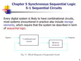
Introduction • The circuits considered thus far have been combinational • The output depends only on the current inputs. • Most systems in practice include storage elements. • Sequential logic.
Sequential Circuits • It consists of: • Combinational circuit. • Storages element. • Storage elements are devices capable of storing binary information. • The binary information stored in these elements at any given time defines the state of the SC at that time.
Sequential Circuits • The SC receives binary information from: • External input. • Present/Current state of storage element. • The next state in the storage element is a function of: • External input. • Present/Current state. • The SC is specified by a time sequence of inputs, outputs, and internal states. Next State Current State
Sequential Circuits • Two main types of SC according to the timing of their signals: • Synchronous SC: • The activity within the circuit and the resulting updating of stored values is synchronized to the occurrence of clock pulses. • Asynchronous SC: • Depends upon the input signals at any instant of time and the order in which the inputs change. • Difficult to design.
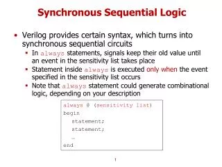
Synchronous Sequential Circuits • Synchronization is by timing device called clock generator clock signal (denoted by clock or clk) periodic train of clock pulses. • Storage elements are affected only with the arrival of each pulse. • In clocked SC: • The clock signal determine whenchanges will occur. • The other signals (e.g. inputs ) determine what are the changes that affect storage elements.
Clock Signal • A sequence of 1s and 0s (ON and OFF periods) Positive edge Transition (rising edge) Positive pulses/level 1 0 Negative edge Transition (falling edge) Negative pulses/level
Storage Element What exactly is memory ? • A memory should support at least three operations. • It should be able to hold a value. • We should be able to read the value that is • saved. • We should be able to change that value.
One Bit Storage Elements • It should be able to hold a single bit, 0 or 1. • We should be able to read the bit that is saved. • We should be able to change the bit. • can set the bit to 1 • can reset or clear the bit to 0.
Storage Element • The momentary change in the storage element state is called a trigger. • Two types of triggering: • Pulse-triggered (Level-Sensitive) • Edge-triggered • Positive edge-triggered (from 0 to 1) • Negative edge-triggered (from 1 to 0) • Main difference between storage elements: • Number of inputs they have. • How the inputs affect the binary state.
Storage Element • Two main types of storage elements: • Latches • Operate with signal levels. • Called level-sensitive. • Not practical for use in synchronous sequential circuits • Flip-Flops • Controlled by clock transition. • Called edge-sensitive. • Flip-Flips are built with latches • Used in clocked SC.
Latches • A latch is binary storage element • Can store a 0 or 1 • It is the most basic storage element. • It is easy to build. • The trigger of a latch start as soon as the clock pulse changes to the logic-1 level. • The new state of a latch appears at the output while the pulse is still active. • Latches respond to new input values as clock pulse is still at logic-1 level.
Latches Types • SR Latch • Latch with Set and Reset inputs implemented with NOR gates • ŚŔ Latch • Same as SR latch except it is implemented with NAND gates • Clocked SR Latch • SR with additional control input (clock) • D Latch • An enhanced storage element from SR Latch with Data input
1- Basic S-R Latches • Two input S(set) R(rest) and Two output Q and Q’ • The S-R latch input will let us control the outputs Q and Q’. • Q and Q’ feed back into the circuit, so they’re not only outputs, they’re also inputs! • To figure out how Q and Q’ change, we must look at not only the inputs S and R, but also the current values of Q and Q’. • Q next = (R + Q’current)’ • Q’next = (S + Qcurrent)’
1- What if S = 0 and R = 0 • The equations on the right reduce to: • Q next= (0 + Q’ current)’= Q current • Q’ next= (0 + Q current)’= Q’ current • So when SR = 00, then Qnext= Qcurrent. • This is exactly what we need tostore • values in the latch.
1- Resetting the latch: SR = 01 • Since R = 1, Qnext is 0, regardless of Qcurrent. Qnext= (1 + Q’current)’ = 0 • Then this new value of Q goes into the bottom NOR gate, where S = 0. Q’next= (0 + 0)’ = 1 • So when SR = 01, then Q next= 0 and Q’next= 1. This is how you reset, or clear, the latch to 0; the R input stands for “reset.”
1- Setting the latch: SR = 10 • What if S = 1 and R = 0? • Since S = 1, Q’next is 0, regardless of Qcurrent. Q’next= (1 + Qcurrent)’ = 0 • Then this new value of Q’ goes into the top NOR gate, along with R = 0. Qnext= (0 + 0)’ = 1 • So when SR = 10, then Q’next= 0 and Qnext= 1. • This is how we set the latch to 1; the S input stands for “set.”
1- SR latches are memories! • This characteristic table shows that our latch provides everything we need in a memory: we can set it, reset it, or keep the current value. • The output Q represents the data stored in the latch. It is also called the state of the latch. • We can expand the table above into a state table, which explicitly shows that the next values of Q and Q’ depend on their current values, as well as on the inputs S and R.
1- What about SR = 11? • Both Q next and Q’ next would become 0, which contradicts the assumption that Q and Q’ are always complements. • SR =11 is avoided
2- S’ R’ Latches (SR Latch with NAND Gate) • Similar to SR latch ( but it is complemented) • Two states: Reset (Q = 0; Q`=1) and set (Q = 1; Q`=0) • When S=R=1, Q remains the same • S=R=0 is not allowed!
3- SR Latch with Clock • The basic SR latch with an additional control input (clock) • determines when the state of the latch can be changed.
3- SR Latch with Clock • It consists of the basic SR latch with two additional NAND gates. • The control input C acts as an enable signal to the latch • When C=0, the S and R inputs have no effect on the latch, so the latch will remain in the same state regardless of the values of S and R. • When C=1, the S and R inputs will have the same effect as in the basic SR latch
4- D Latch • One way to eliminate the undesirable undefined state in the SR latch is to ensure that the inputs S and R are never equal to 1 at the same time.
4- D Latch • Adding an inverter to the S-R Latch, gives the D Latch • Ensure S and R are never equal to 1 at the same time • Add inverter • Only one input (D) • D connects to S • D’ connects to R • D stands for data • Output follows the input when C = 1 • Transparent • When C = 0, Q remains the same
Generally, Latches • A latch is designated by a rectangular block with inputs on the left and outputs on the right • One output designates the normal output, the other (with the bubble) designates the complement • For S’R’ (SR built with NANDs), bubbles added to the input
Flip-Flop • The problem with the latch is that it responds to a change during a positive level (or a negative level) of a clock pulse but in a sequential circuit we need to trigger the element only at a signal transition instant.
D Flip-Flop • The most economical FF because it need smallest number of gates between all FF types. • Two different ways to construct a D flip-flop from latches are here. • Master-slave D flip-flop is shown below
D Flip-Flop • Timing diagram example( rising edge): Clock D Q
D Flip-Flop More efficient construction (using threeSR latches) • CLK = 0 ,S and R are equal to 1 (which causes no change in the output) • CLK becomes 1: • If D = 0 , R changes to 0 (Since S = 1) and this resets the flip-flop, making Q = 0 • Now if D changes its value (while CLK = 1), since R = 0, it will not change the value of R. • CLK becomes 0, • R goes to 1 which is a normal condition (as S is still 1), causing no change in the output. • CLK goes from 0 ( previous step )to 1 • D = 1 when, set state.
JK Flip-Flop • The indeterminate condition of the SR type is defined in the JK type. • It can set/reset/complement the output. • Characteristics table: • Characteristics equation: Q(t+1)= JQ’+K’Q
JK Flip-Flop • Timing diagram example( rising edge): Clock J K Q
T Flip Flop • ×خ
T Flip-Flop • Timing diagram example( rising edge): Clock T Q
Direct Inputs • Flip Flops will sometimes provide special input terminals for setting or clearing the FF asynchronously. • Direct inputs force FF to a state independently of clock. • The input that sets FF to 1 is called preset or direct set. • The input that resets FF to 0 is called clear or direct reset. • These inputs are useful for bringing the FFs to an initial state prior to its clocked operation.
Excitation Table • In the design process: • We know the transition from the present state to the next state. • Want to find the FF inputs that cause the transition. • To achieve the goal of design we need Excitation Table. • A table that lists the required inputs for a given change of state. D 0 1
FF Summery • Three types of Flip Flop: • D Flip Flop(FF) • consider the basic and more efficient. • Other FF can be constructed using it. • 1 input (D), and can Set/Reset output. • JK FF. • Constructed with D FF and gates. • 2 inputs (J,K) and can Set/Rest / Complement the output. • T FF • Constructed with D FF and XOR gate • 1 input( T) and can implement the output.