Download
1 / 76
820 likes | 1.17k Views
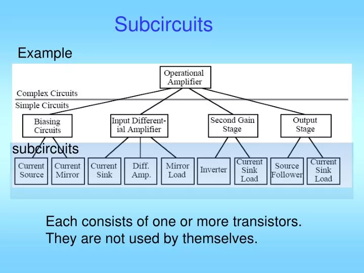
Subcircuits. Example. subcircuits. Each consists of one or more transistors. They are not used by themselves. Subcircuits. Switches Diodes/active resistors Current mirrors Current sources/current sinks Current/voltage references Band gap references. MOS switches. Ideal Switch.

E N D
Subcircuits Example subcircuits Each consists of one or more transistors. They are not used by themselves.
Subcircuits • Switches • Diodes/active resistors • Current mirrors • Current sources/current sinks • Current/voltage references • Band gap references
MOS switches Ideal Switch MOS transistor as a switch
RON Simple approximation On operation: VG >> VS or VD, VDS small, triode A B Off operation: VGS < VT , cutoff A B Very good off-char
Observations: • RON depends on W, L, VG, VT, VDS, etc • RON is nonlinear (depending on signal) Want: RON small and constant Strategies: • Use large W and small L to reduce RON • Use large VGS to reduce the effect of signal dependency • Use bootstrapping to increase VGS beyond VDD–VSS • Use constant VGS • Use constant VB so as to have fixed VT
Effects of switch non-idealities • Finite ON Resistance • Non-zero charging and discharging time • Limit settling • Limits conversion rate Actually: takes time Ideally: instantaneous charging
Signal level dependence of RON • Different settling behavior at different signal levels • Introduces nonlinearity • Generate higher order harmonics Vin: pure sine wave VC1: has harmonic distortions
Finite OFF Current • Leakage of a held voltage • Coupling through the switch • Accumulates with time
EXAMPLE - Switched Capacitor Integrator (slow clock edge) Assume:
At t2: At t3: Once M2 turns on at t3, all charge on C1 is transferred to C2
Between t3 and t4 additional charge is transferred to C1 from the channel capacitance of M2. At t4: Ideal transfer: Total error:
Charge injection When switch is turned off suddenly, charges trapped in the channel injected both either D and S side equally. The amount of trapped charges depends on the slope of VG
=U slow regime: L Hold value error on CL:
In the fast edge regime: Hold voltage error on CL: Study the example in the book
Dummy transistor to cancel clock feed through Complete cancellation is difficult. Requires a complementary clock.
Use CMOS switches Advantages - 1.) Larger dynamic range. 2.) Lower ON resistance. Disadvantages - 1.) Requires complementary clock. 2.) Requires more area.
Constant VGS Bootstrapping f=0 f=1 VG=0 VDD VGS~VDD
When f=1: Cp: total parasitic capacitance connected to top plate of C3.
on off PMOS version
Concept: Switched cap implementation
Summary on Switches • To reduce RON • Use large W and small L • Use CMOS instead of NMOS or PMOS • Use large |VGS| • To reduce clock feed through • Use cascode • Use dummy transistor • To reduce charge injection • Use dummy • Use slow clock edge • Use complementary clock on switch and dummy • To improve linearity • Use large |VGS| • Use vin-independent VGS • Use vin-independent VBS (PMOS switch)
Diodes And Active Resistors • Simple diode connection • Voltage divider • Extending the dynamic range • Parallel MOSFET resistor • Extending the dynamic range • Differential resistor • Single MOSFET • Double MOSFET
Diode Connection VDS = VGS Always in saturation If v > VT, i > 0 else i = 0 diode i v VT
Generally, gm≈ 10 gmbs ≈ 100 gds If VBS=0,
Voltage Division Equating iD1 to iD2 results in: VDS1 +VDS2 = VDD - VSS Can use different W/L ratio to achieve desired voltage division Use less power than resistive divider
Active vs passive resistors Suppose Vo=(VDD+VSS)/2 =2 gm1=gm2=bVEB=10*0.2=2 m Ro=1/4m = 250 ohm Ro Io=b/2 *(VEB)2=0.2mA =0 To achieve the same Ro, need two 500 ohm resistors. Io=2/(2*500)=2mA, 10 times Ro Consumes 10 times more power
Current sources / sinks V Current source I I Current sink V I V
Two critical figures of merit How flat the operating portion is How small the non-operating region is rout and vmin For the simple sink on prev slide:
Very flat Too large
Reduction of VMIN rout≈ rds1*gm2rds2 is large which is good But vmin = vT +2VON needs to be reduced
Both just saturating But the 2 IREFs must be the same. How?
M6 is ¼ the size, it requires 2 times over drive, or 2 times VEB, or 2 time VON Very flat VMIN is much smaller
Alternative method M5 is ¼ the size Again, the 2 IREFs must be the same.
VON≈ 0.6V Larger W/L ratio can significantly reduce VON
Matching Improved by Adding M3 Why is it better now?
Regulated Cascode Current Sink Near triode, VDS3↓, iout↓, VGS4 ↓, VD4 or VG5 ↑, Iout ↑.
HW: • As we pointed out, the circuit on the previous page suffers from a large Vmin. • Modify the circuit to reduce Vmin without affecting rout. • Once you do that, VDS for M1 and M2 are no longer match. Introduce another modification so that the VDSs are matched.
Simple Current Mirrors Assuming square law model: