Download
1 / 60
600 likes | 771 Views
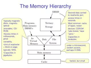
The Memory Hierarchy. Instructor: Dr. Hyunyoung Lee Based on slides provided by Randy Bryant and Dave O’Hallaron. Today. Storage technologies and trends Locality of reference Caching in the memory hierarchy. Random-Access Memory (RAM). Key features RAM is packaged as a chip.

E N D
The Memory Hierarchy Instructor: Dr. Hyunyoung Lee Based on slides provided by Randy Bryant and Dave O’Hallaron
Today • Storage technologies and trends • Locality of reference • Caching in the memory hierarchy
Random-Access Memory (RAM) • Key features • RAM is packaged as a chip. • Basic storage unit is a cell (one bit per cell). • Multiple RAM chips form a memory. • Static RAM (SRAM) • Each cell stores a bit with a six-transistor circuit. • Retains value indefinitely, as long as it is kept powered. • Relatively insensitive to disturbances such as electrical noise (EMI). • Faster and more expensive than DRAM. • Dynamic RAM (DRAM) • Each cell stores bit with a capacitorand a transistor. • Value must be refreshed every 10-100 ms. • More sensitive to disturbances (EMI, radiation,…) than SRAM. • Slower and cheaper than SRAM.
SRAM vs DRAM Summary Trans. Access Needs per bit time refresh? Sensitive? Cost Applications SRAM 6 1X No No 100x Cache memories DRAM 1 10X Yes Yes 1X Main memories, frame buffers of graphics system
Conventional DRAM Organization • dxw DRAM: • dw total bits organized as dsupercells of size w bits 16 x 8 DRAM chip cols 0 1 2 3 Memory controller 0 2 bits / addr 1 rows supercell (2,1) 2 (to/from CPU) 3 8 bits / data Internal row buffer
Reading DRAM Supercell (2,1) Step 1(a): Row access strobe (RAS) selects row 2. Step 1(b): Row 2 copied from DRAM array to row buffer. 16 x 8 DRAM chip Cols 0 Memory controller 1 2 3 RAS = 2 2 / 0 addr 1 Rows 2 3 8 / data Internal row buffer
supercell (2,1) supercell (2,1) Reading DRAM Supercell (2,1) Step 2(a): Column access strobe (CAS) selects column 1. Step 2(b): Supercell (2,1) copied from buffer to data lines, and eventually back to the CPU. 16 x 8 DRAM chip Cols 0 Memory controller 1 2 3 CAS = 1 2 / 0 addr To CPU 1 Rows 2 3 8 / data Internal row buffer
addr A (row = i, col = j) bits 56-63 bits 48-55 bits 40-47 bits 32-39 bits 24-31 bits 16-23 bits 8-15 bits 0-7 63 63 56 56 55 55 48 48 47 47 40 40 39 39 32 32 31 31 24 24 23 23 16 16 15 15 8 8 7 7 0 0 64-bit doubleword at main memory address A 64-bit doubleword to CPU chip Memory Modules (plugged into expansion slots on the motherboard) : supercell (i,j) DRAM 0 64 MB memory module consisting of eight 8Mx8 DRAM chips DRAM 7 Memory controller
Enhanced DRAMs • Basic DRAM cell has not changed since its invention in 1966. • Commercialized by Intel in 1970. • All enhancements are built around the conventional DRAM core. • DRAM cores with better interface logic and faster I/O : • Fast page mode DRAM (FPM DRAM) • Reuse of the row address [RAS, CAS, CAS, CAS] instead of [(RAS,CAS), (RAS,CAS), (RAS,CAS)] • Synchronous DRAM (SDRAM) • Uses rising clock edge signal instead of asynchronous control signals • Double data-rate synchronous DRAM (DDR SDRAM) • Double edge clocking sends two bits per cycle per pin • By 2010, standard for most server and desktop systems • Video RAM (VRAM) • Like FPM DRAM, but output is produced by shifting row buffer • Dual ported (allows concurrent reads and writes)
Nonvolatile Memories • DRAM and SRAM are volatile memories • Lose information if powered off. • Nonvolatile memories retain value even if powered off • Generic name is read-only memory (ROM). • Misleading because some ROMs can be modified. • Types of ROMs • Programmable ROM (PROM): can be programmed once • Eraseable PROM (EPROM): can be bulk erased (UV, X-Ray) • Electrically eraseable PROM (EEPROM): electronic erase capability • Flash memory: EEPROMs with partial (sector) erase capability • Wears out after about 100,000 erasings. • Uses for Nonvolatile Memories • Firmware programs stored in a ROM (BIOS, controllers for disks, network cards, graphics accelerators, security subsystems,…) • Solid state disks (replace rotating disks in thumb drives, smart phones, mp3 players, tablets, laptops,…)
Traditional Bus Structure Connecting CPU and Memory • A bus is a collection of parallel wires that carry address, data, and control signals. • Buses are typically shared by multiple devices. CPU chip Register file ALU System bus Memory bus Main memory Bus interface I/O bridge
Memory Read Transaction (1) • CPU places address A on the memory bus. Register file Load operation:movl A, %eax ALU %eax Main memory 0 I/O bridge A Bus interface A x
Memory Read Transaction (2) • Main memory reads A from the memory bus, retrieves word x, and places it on the bus. Register file Load operation:movl A, %eax ALU %eax Main memory 0 I/O bridge x Bus interface A x
Memory Read Transaction (3) • CPU reads word x from the bus and copies it into register %eax. Register file Load operation:movl A, %eax ALU %eax x Main memory 0 I/O bridge Bus interface A x
Memory Write Transaction (1) • CPU places address A on bus. Main memory reads it and waits for the corresponding data word to arrive. Register file Store operation:movl %eax, A ALU %eax y Main memory 0 I/O bridge A Bus interface A
Memory Write Transaction (2) • CPU places data word y on the bus. Register file Store operation:movl %eax, A ALU %eax y Main memory 0 I/O bridge y Bus interface A
Memory Write Transaction (3) • Main memory reads data word y from the bus and stores it at address A. register file Store operation:movl %eax, A ALU %eax y main memory 0 I/O bridge bus interface A y
What’s Inside A Disk Drive? Spindle Arm Platters Actuator Electronics (including a processor and memory!) SCSI connector Image courtesy of Seagate Technology
Disk Geometry • Disks consist of platters, each with two surfaces. • Each surface consists of concentric rings called tracks. • Each track consists of sectors separated by gaps. Tracks Surface Track k Gaps Spindle Sectors
Disk Geometry (Muliple-Platter View) • Aligned tracks form a cylinder. Cylinder k Surface 0 Platter 0 Surface 1 Surface 2 Platter 1 Surface 3 Surface 4 Platter 2 Surface 5 Spindle
Disk Capacity • Capacity: maximum number of bits that can be stored. • Vendors express capacity in units of gigabytes (GB), where1 GB = 109 Bytes (Lawsuit pending! Claims deceptive advertising). • Capacity is determined by these technology factors: • Recording density (bits/in): number of bits that can be squeezed into a 1 inch segment of a track. • Track density (tracks/in): number of tracks that can be squeezed into a 1 inch radial segment. • Areal density (bits/in2): product of recording and track density. • Modern disks partition tracks into disjoint subsets called recording zones • Each track in a zone has the same number of sectors, determined by the circumference of innermost track. • Each zone has a different number of sectors/track
Computing Disk Capacity Capacity = (# bytes/sector) x (avg. # sectors/track) x (# tracks/surface) x (# surfaces/platter) x (# platters/disk) Example: • 512 bytes/sector • 300 sectors/track (on average) • 20,000 tracks/surface • 2 surfaces/platter • 5 platters/disk Capacity = 512 x 300 x 20000 x 2 x 5 = 30,720,000,000 = 30.72 GB
The read/write head is attached to the end of the arm and flies over the disk surface on a thin cushion of air. By moving radially, the arm can position the read/write head over any track. Disk Operation (Single-Platter View) The disk surface spins at a fixed rotational rate spindle spindle spindle spindle spindle
Disk Operation (Multi-Platter View) Read/write heads move in unison from cylinder to cylinder Arm Spindle
Surface organized into tracks Tracks divided into sectors Disk Structure - top view of single platter
Disk Access Head in position above a track
Disk Access Rotation is counter-clockwise
Disk Access – Read About to read blue sector
Disk Access – Read After BLUEread After reading blue sector
Disk Access – Read After BLUEread Red request scheduled next
Disk Access – Seek After BLUEread Seek for RED Seek to red’s track
Disk Access – Rotational Latency After BLUEread Seek for RED Rotational latency Wait for red sector to rotate around
Disk Access – Read After BLUEread Seek for RED Rotational latency After RED read Complete read of red
Disk Access – Service Time Components After BLUEread Seek for RED Rotational latency After RED read Data transfer Seek Rotational latency Data transfer
Disk Access Time • Average time to access some target sector approximated by : • Taccess = Tavg seek + Tavg rotation + Tavg transfer • Seek time (Tavg seek) • Time to position heads over cylinder containing target sector. • Typical Tavg seek is 9 ms • Rotational latency (Tavg rotation) • Time waiting for first bit of target sector to pass under r/w head. • Tavg rotation = 1/2 x 1/RPMs x 60 sec/1 min • Typical Tavg rotation = 7200 RPMs • Transfer time (Tavg transfer) • Time to read the bits in the target sector. • Tavg transfer = 1/RPM x 1/(avg # sectors/track) x 60 secs/1 min.
Disk Access Time Example • Given: • Rotational rate = 7,200 RPM • Average seek time = 9 ms. • Avg # sectors/track = 400. • Derived: • Tavg rotation = 1/2 x (60 secs/7200 RPM) x 1000 ms/sec = 4 ms. • Tavg transfer = 60/7200 RPM x 1/400 secs/track x 1000 ms/sec = 0.02 ms • Taccess = 9 ms + 4 ms + 0.02 ms • Important points: • Access time dominated by seek time and rotational latency. • First bit in a sector is the most expensive, the rest are free. • SRAM access time is about 4 ns/doubleword, DRAM about 60 ns • Disk is about 40,000 times slower than SRAM, • 2,500 times slower then DRAM.
I/O Bus CPU chip Register file ALU System bus Memory bus Main memory Bus interface I/O bridge I/O bus Expansion slots for other devices such as network adapters. USB controller Graphics adapter Disk controller Mouse Keyboard Monitor Disk
Reading a Disk Sector (1) CPU chip CPU initiates a disk read by writing a command, logical block number, and destination memory address to a port (address) associated with disk controller. Register file ALU Main memory Bus interface I/O bus USB controller Graphics adapter Disk controller keyboard mouse Monitor Disk
Reading a Disk Sector (2) CPU chip Disk controller reads the sector and performs a direct memory access (DMA) transfer into main memory. Register file ALU Main memory Bus interface I/O bus USB controller Graphics adapter Disk controller Mouse Keyboard Monitor Disk
Reading a Disk Sector (3) CPU chip When the DMA transfer completes, the disk controller notifies the CPU with an interrupt (i.e., asserts a special “interrupt” pin on the CPU) Register file ALU Main memory Bus interface I/O bus USB controller Graphics adapter Disk controller Mouse Keyboard Monitor Disk
Storage Trends SRAM Metric 1980 1985 1990 1995 2000 2005 2010 2010:1980 $/MB 19,200 2,900 320 256 100 75 60 320 access (ns) 300 150 35 15 3 2 1.5 200 DRAM Metric 1980 1985 1990 1995 2000 2005 2010 2010:1980 $/MB 8,000 880 100 30 1 0.1 0.06 130,000 access (ns) 375 200 100 70 60 50 40 9 typical size (MB) 0.064 0.256 4 16 64 2,000 8,000 125,000 Disk Metric 1980 1985 1990 1995 2000 2005 2010 2010:1980 $/MB 500 100 8 0.30 0.01 0.005 0.0003 1,600,000 access (ms) 87 75 28 10 8 4 3 29 typical size (MB) 1 10 160 1,000 20,000 160,000 1,500,000 1,500,000
CPU Clock Rates Inflection point in computer history when designers hit the “Power Wall” 1980 1990 1995 2000 2003 2005 2010 2010:1980 CPU 8080 386 Pentium P-III P-4 Core 2 Core i7 --- Clock rate (MHz) 1 20 150 600 3300 2000 2500 2500 Cycle time (ns) 1000 50 6 1.6 0.3 0.50 0.4 2500 Cores 1 1 1 1 1 2 4 4 Effective cycle 1000 50 6 1.6 0.3 0.25 0.1 10,000 time (ns)
The CPU-Memory Gap The gap widens between DRAM, disk, and CPU speeds. Disk SSD DRAM CPU
Locality to the Rescue! The key to bridging this CPU-Memory gap is a fundamental property of computer programs known as locality
Today • Storage technologies and trends • Locality of reference • Caching in the memory hierarchy
Locality • Principle of Locality:Programs tend to use data and instructions with addresses near or equal to those they have used recently • Temporal locality: • Recently referenced items are likely to be referenced again in the near future • Spatial locality: • Items with nearby addresses tend to be referenced close together in time
Locality Example • Data references • Reference array elements in succession (stride-1 reference pattern). • Reference variable sum each iteration. • Instruction references • Reference instructions in sequence. • Cycle through loop repeatedly. sum = 0; for (i = 0; i < n; i++) sum += a[i]; return sum; Spatial locality Temporal locality Spatial locality Temporal locality
Qualitative Estimates of Locality • Claim: Being able to look at code and get a qualitative sense of its locality is a key skill for a professional programmer. • Question: Does this function have good locality with respect to array a? intsum_array_rows(inta[M][N]) { inti, j, sum = 0; for (i = 0; i < M; i++) for (j = 0; j < N; j++) sum += a[i][j]; return sum; }
Locality Example • Question: Does this function have good locality with respect to array a? intsum_array_cols(inta[M][N]) { inti, j, sum = 0; for (j = 0; j < N; j++) for (i = 0; i < M; i++) sum += a[i][j]; return sum; }
Locality Example • Question: Can you permute the loops so that the function scans the 3-d array a with a stride-1 reference pattern (and thus has good spatial locality)? int sum_array_3d(int a[M][N][N]) { inti, j, k, sum = 0; for (i = 0; i < M; i++) for (j = 0; j < N; j++) for (k = 0; k < N; k++) sum += a[k][i][j]; return sum; }