Download
1 / 58
640 likes | 1k Views
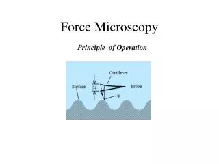
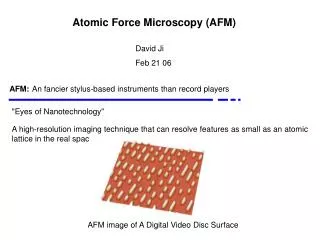
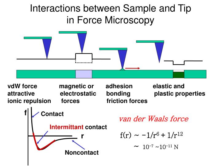
Interactions between Sample and Tip in Force Microscopy. vdW force magnetic or adhesion elastic and attractive electrostatic bonding plastic properties ionic repulsion forces friction forces. f. Contact.

E N D
Interactions between Sample and Tipin Force Microscopy vdW force magnetic or adhesion elastic and attractive electrostatic bonding plastic properties ionic repulsion forces friction forces f Contact van der Waals force Intermittant contact f(r) ~ -1/r6 +1/r12 r ~ 10-7 ~10-11 N Noncontact
Force vs. Distance Vacuum touching untouch Air Capillary force Pull off Slope: elastic modulus of soft sample or force constant k of cantilever Contamnated in air
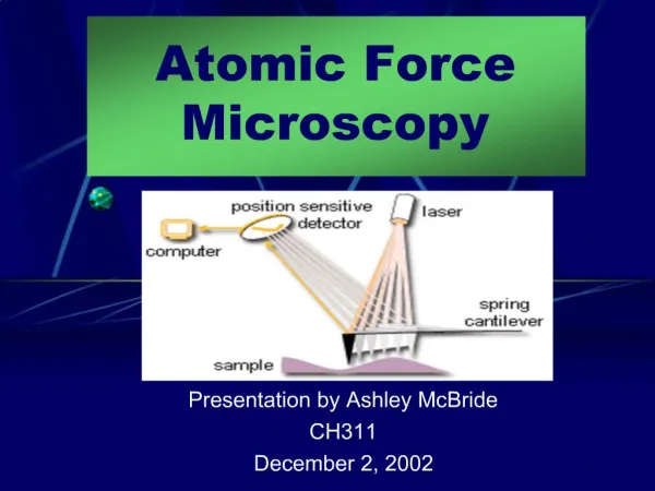
Atomic Force Microscope (AFM) • Sample: conductor, nonconductor, etc • Force sensor: cantilever • Deflection detection: photodiode interferometry (10-4A)
Contact strong (repulsive): constant force or constant distance Noncontact weak(attractive): vibrating probe Intermittent contact strong(repulsive): vibrating probe Lateral force frictional forces exert a torque on the scanning cantilever Magnetic force the magnetic field of the surface Thermal scanning the distribution of thermal conductivity Mode of Operation Force of interaction
Force Sensor: Cantilever • Material: Si,Si3N4 • Dimension: • Stiffness • - soft: contact mode • - stiff: vibrating (dynamic force) • mode • Spring constant (k): • 0.1-10N/m • Resonance frequency: 10~100kHz 100-200 mm 1-4 mm 10 mm ~20nm From DI
Scanning Modes Contact Noncontact Vibrating (tapping) Cantilever soft hard hard Force 1-10nN 0.1-0.01nN Friction large small small Distance <0.2nm ~ 1nm >10nm Damage large small small Polymer latex particle on mica From DI
Vibrating Cantilever (tapping) Mode • Vibration of cantilever around its resonance frequency • Change of frequency (fo) due to interaction between sample • and cantilever Resonance Frequency keff = k0 - dF/dz feff = 2p(keff /m)1/2 • Amplitude imaging • Phase imaging • Removal of lateral force contribution
Image Artifacts • Tip imaging • Feedback artifacts • Convolution with other physics • Imaging processing • How to check ? • Repeat the scan • Change the direction • Change the scan size • Rotate the sample • Change the scan speed AFM image of random noise. Left image is raw data. Right image is a false image, produced by applying a narrow bandpass filter to the raw data www.psia.co.kr/appnotes/apps.htm
Applications of SPM • Surface morphology, especially for insulators • Lateral, adhesion, molecular and magnetic forces • Temperature, capacitance, and surface potential • mapping • Nano-lithography • Surface modification and manipulation • Imaging of biomolecules, and polymers
STM and AFM Images of Co-Nanoparticles STM: on H/Si(111) AFM: on HOPG TEM: on Carbon grid Co-nanoparticle stripes prepared By Mirco Contact Printing AFM image UHV-STM image (200 nm x 200 nm) after annealing under 500 C S.S.Bae et al (2001)
Force Measurement of DNA strands Baselt et al, J. Vac. Sci. Tech. B14, 789 (1996)
Manipulation of Nanoparticles by AFM Ref 15 in G.S. McCarth and P.S.Weiss, Chem. Rev. 99, 1983 (1999)
AFM-tip-induced Local Oxidation on Si Ph. Avouris et al, App. Phys. A 66, S659 (1998)
Lateral Force Microscopy Laterally twisted due to friction High resolution topography (top) and Lateral Force mode (bottom) images of a commercially avail-able PET film. The silicate fillers show increased friction in the lateral force image. www.tmmicro.com/tech/modes/lfm.htm
Force Modulation Micrscopy • Contact AFM mode • Periodic signal is applied to either to tip or sample • Simultaneous imaging of topography and material properties • Amplitude change due to elastic properties of the sample PSIA, www.psia.co.kr/appnotes/apps.htm
Phase Detection Microscopy • Intermittant-contact AFM mode • Monitoring of phase lag between the signal drives • the cantilever and the catilever oscillation signal • Simultaneous imaging of topography and material properties • Change in mechanical properties of sample surface
Chemical Force Microscopy CH3 COOH • topography • friction force using a tip modified with a COOH-terminated SAM, • frinction force using a tip modified with a methyl-terminated SAM. • Light regions in (B) and (C) indicate high friction; dark regions indicate low frinction. A. Noy et al, Ann. Rev. Mater. Sci. 27, 381 (1997)
Magnetic Force Microscopy Glass Hard Disk Sample AFM image MFM image • Ferromagnetic tip: Co, Cr • Noncontact mode • vdW force: short range force • Magnetic force: long range force; small force gradient • Close imaging: topography • Distant imaging: magnetic properties http://www.tmmicro.com/tech/index.htm
Scanning Kelvin Probe Microscopy (SKPM) Scanning Tunneling Potentiometry (STP) Scanning Maxwell Microscopy (SMM) Electrostatic Force Microscopy(EFM) Metallic tip Bias Voltage • Ferroelectric materials • Charge distribution on surfaces • Failure analysis on the device http://www.tmmicro.com/tech/index.htm
Theory of EFM • Electrostatic force bewteen sample and tip • F = Fcapacitance + F coulomb (Fcapacitance = dEc /dz , Ec = CV2/2) • = (1/2)V2(dC/dz) + (1/4pe z2)QsQt • = (1/2) (dC/dz) (Vdc +Vac cos wt)2 • - (1/4pe z2)Qs (Qs +CVdc +CVac cos wt) • = (1/2) (dC/dV) (V 2dc + (1/2) Vac2 ) - (1/4pe z2)Qs (Qs +CVdc) • + (2VdcdC/dz - Qs C /4pe z)Vaccos wt • + (1/4)dC/dzV 2accos 2wt • Ist harmonic term: Surface potential (Vdc ), surface charge (Qs) • 2nd harmonic term: dC/dz doping concentration
Scanning Capacitance Microscopy (SCM) Transistor Oxide Thickness Metallic tip Contact Topograph SCM • LC capacitance circuit • Doping concentration • Local dielectric constant http://www.psia.co.kr/appnotes/apps.htm
Scanning Thermal Microscopy • Subsurface defect review • Semiconductor failure analysis • Measure conductivity differences in copolymers, • surface coatings etc
Hybrid Tools: AFM inside SEM M.F. Yu et al, Nanotechnology10, 244 (1999)
Nearfield Scanning Optical Microscopy Topography and Optical properties Glass hv Detector Al f=60-200nm d Fluorescence image of a single DiIC molecule. Image courtesy of P. Barabara/Dan Higgins • Near field: d<<l • Resolution ~ d andf • Approach: shear force http://www.psia.co.kr/data/nsom.htm
Scanning Electrochemical Microscopy Electrochemistry Surface structure Electrochemical deposition Corrosion From J. Kwak
A A FEEDBACK Photon Emission STM Photon detector Local chemical environment G.S. McCarty and P.S. Weiss, Chem. Rev. 99, 1983 (1999)
. . A A Ballistic Electron . . A FEEDBACK FEEDBACK BEEM (Ballistic Electron Emission Microscopy) Ef gap Tip BaseCollector(Si) STP (Scanning Tunneling Potentiometry)
Summary • SPM haseyes to see the geometry and properties of nanostructures and fingers to manipulate and build nanostructures
3. 전자 분광학의 원리 및 응용 • IMFP of electron • Auger electron spectroscopy • Photoelectron spectroscopy • - Koopmann’s theorem • - Chemical shift • - Spin-orbit coupling etc • 4. Microscopies: PEEM, LEEM, Imaging XPS • References: • 1. Electron spectroscopy, theory, techniques, and applications I-IV, • edited by C.R. Brundle (Academic, NY, 1977) • 2. G. Ertl and J. Kuppers, Low energy electrons and surface chemistry (VCH, 1985) • 3. Practical surface analysis, I,II, edited by D. Briggs and M.P.Seah (Salle & • Sauerlander) • 4. S. Hufers, Photoelectron spectroscopy, in Springer series in sol. state phys. v 82 • 5. Internet lecture: http://www.chem.qmw.ac.uk/surfaces/#teach
Electron Spectroscopies • Auger Electron Spectroscopy (AES) • X-ray Photoelectron Spectroscopy (ESCA) • Ultraviolet Photoelectron Spectroscopy (UPS) • Electron Energy Loss Spectroscopy (EELS) • High Resolution EELS • Electron Microscopies • Scanning Auger Microscopy (SAM) • Photoemission Electron Microscopy (PEEM) • Low Energy Electron Microscopy (LEEM) • Scanning X-ray Photoelectron Microscopy • (SXPEM) • Secondary Electron Microscopy with • Polarization Analysis (SEMPA) Acronyms
Why are electron spectroscopies surface sensitive ? 100 IMFP(nm) 10 1 0 • 10 100 1000 10000 • Energy (eV) The inelastic mean free path (IMFP) of electrons is less than 1 nm for electron energies with 10~1000 eV.
Auger Electron Spectroscopy Auger electron e L23 L1 K hv or e e KE = EK– EL1– EL23 Kinetic Energy of Auger Electrons for KLL Transition Element Specific
Applicatons • Chemical identification: 1% monolayer • Quantitative analysis • Auger depth profiling • Scanning Auger Microscopy (SAM) • - Spatially-resolved compositional • information
SEM and SAM Focused electron gun Detector SiC grain size = 0.04 m Secondary electrons SEM topograph of Au-SiC codeposits Energy Analyser Auger electrons SAM image of Ag particles (d=1nm)
Photoelectron Spectroscopy X-ray Photoelectron Spectroscopy (XPS): hv=200~2000 eV Ultraviolet Photoelectron Spectroscopy (UPS): hv =10~50 eV photoelectron KE KE: kinetic energy BE: binding energy F: work function hn(E,p,q) e(E,q,s) Ev f Ef hn BE KE = hn– BE - f
Photoemission peak intensity I(E, hv) ~ Nv(E) Nc(E) s(E,hv): UPS limit ~ Nv(E)s(E,hv): XPS limit, where Nv(E): densities of initial states(i) Nc(E): densities of final states(f) s(E,hv): photoionization cross section s~ |<f|AP|i>|2 The XPS spectra represent the total density-of-states modulated by the cross-section for photoemission
Koopman’s Theorem: frozen orbital approximation A(N) + hv A+(N-1) + e e hv + e(KE) initial state final state Ei(N) + hv = Ef(N-1) + KE BE = hv –KE = Ef(N-1) - Ei(N) = -eiHF - erelax+ ecorrel BE of core level≈ - eiHF( ith orbital energy)
Chemical Shift of Binding Energy Valence shell Electron charge q r Core electron e The core electron feels an alteration in the chemical environment when a change in the charge of the valence shell occurs. A change in q, dq, gives a potential change dE = e dq/r • the oxidation state of the atom • the chemical environment
Core level Spectra of SiON J.W. Kim et al (2001)
Example of Chemical Shift • The chemical shift: ~4.6 eV • Metals: an asymmetric line shape (Doniach-Sunjic) • Insulating oxides: more symmetric peak
Photoemission features • Spin-orbit splitting • Shake-up and shake off • Multiplet splitting • Plasmon losses Ref: Electron spectroscopy I-IV edited by C.R. Brundle and A.D. baker Photoelectron spectroscopy by S. Hufner
Spin-orbit Coupling Pd: (3d)10+ hv(3d)9+ e L =2 , S = ½, J = L+S,…, L-S = 5/2, 3/2 2D 5/2 g J = 2x{5/2}+1 = 6 2D 3/2 g J = 2x{3/2}+1 = 4
Shake up and shake off: Final state effect • Multi-electronic transitions after creation of Ne 1s core hole • - Excitation of electron to higher bound state: shake up • - Excitation to continuum state: shake off
Multiplet Splitting Fe 3+(3s23d5) + hv Fe 4+(3s13d5) + e 3d 3s Initial state Final state Terms: 6S 7S 5S
Applications • Determination of energy levels • Chemical bonding • Oxidation states • Density-of-states of valence bands • Energy bands • Quantum well states • Quantitative analysis