Download
1 / 31
310 likes | 805 Views
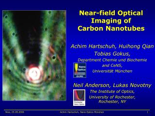
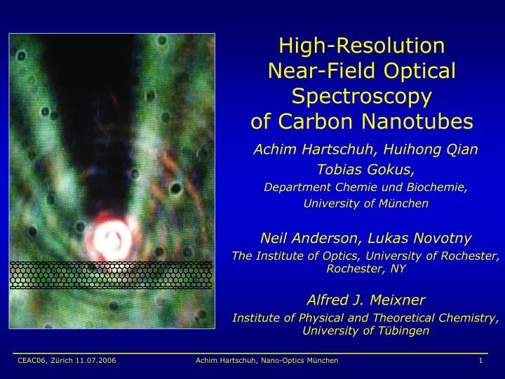
High-Resolution Near-Field Optical Spectroscopy of Carbon Nanotubes. Achim Hartschuh, Huihong Qian Tobias Gokus, Department Chemie und Biochemie, University of München Neil Anderson, Lukas Novotny The Institute of Optics, University of Rochester, Rochester, NY Alfred J. Meixner

E N D
High-Resolution Near-Field Optical Spectroscopy of Carbon Nanotubes Achim Hartschuh, Huihong Qian Tobias Gokus, Department Chemie und Biochemie, University of München Neil Anderson, Lukas Novotny The Institute of Optics, University of Rochester, Rochester, NY Alfred J. Meixner Institute of Physical and Theoretical Chemistry, University of Tübingen Achim Hartschuh, Nano-Optics München
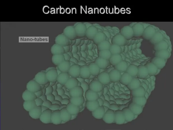
Single-walled Carbon Nanotubes • 1D crystal: • Diameter ~ 0.5-3 nm • Length up to mm • Different structures • (Diameter, chirality) • (n,m) • Structure determines • properties • (n-m) mod 3 = 0 • metallic • else semicond. Graphene sheet + roll up single-walled carbon nanotube S. Maruyama, http://chishiki.t.u-okyo.ac.jp/ ~maruyama/index.html Achim Hartschuh, Nano-Optics München
Why High Spatial Resolution Near-field Optics? Achim Hartschuh, Nano-Optics München
Why Near-field Optics? Achim Hartschuh, Nano-Optics München
spatial resolution is limited by diffraction l/2 Why Near-field Optics? Achim Hartschuh, Nano-Optics München
Uncertainty relation: Diffraction Limit Abbé, Arch. Mikrosk. Anat. 9, 413 (1873) Achim Hartschuh, Nano-Optics München
Tip-Enhanced Spectroscopy Wessel, JOSA B 2, 1538 (1985) Achim Hartschuh, Nano-Optics München
Tip-Enhanced Spectroscopy laser illuminated metal tip Novotny et al. PRL 79, 645 (1997) Theory: (Giant) enhanced electric field confined to tip apex Mechanism: Lightning rod and antenna effect, plasmon resonances Achim Hartschuh, Nano-Optics München
Tip-Enhanced Spectroscopy SEM micrograph diameter = 22 nm • enhanced electric field confined within 20 nm ? ……………….Optical imaging with 20 nm resolution?! ……………….Signal enhancement !? Achim Hartschuh, Nano-Optics München
Tip-Enhanced Spectroscopy tip has to be very close to the sample raster-scanning the sample and point-wise detection of the sample response enhanced electric field close to the very end of the tip Achim Hartschuh, Nano-Optics München
+ Tip-sample distance control a sharp metal tip is held at constant height (~2nm) above the sample using a tuning-fork feedback mechanism. F~10 pN K. Karrai et al., APL 66, 1842 (1995) 2 nm Topography of the sample Experimental Setup Confocal microscope Optical Images and Spectra Achim Hartschuh, Nano-Optics München
Near-field Raman Imaging of SWCNTs Raman image (G’ band) Topography Hartschuh et al. PRL 90, 95503 (2003) 500 nm 500 nm only SWCNT detected in optical image chemically specific optical contrast with 25 nm resolution enhanced field confined to tip Achim Hartschuh, Nano-Optics München
G RBM at 199 cm-1 diam = 1.2 nm structure (n,m)(14,2) metallic SWCNT RBM Near-field Raman Spectroscopy Raman image (G band) Topography image height: 0 - 1.9 nm Anderson et al. JACS 127, 2533 (2005) Hartschuh et al. Int. J. Nanosc. 3, 371 (2004) Achim Hartschuh, Nano-Optics München
Experiment RBM D G Exp. parameters: ~3 nm steps between spectra exposure time per spectrum = 100 ms intensity of the RBM 100 nm Achim Hartschuh, Nano-Optics München
Resolution enhancement Farfield Near-field no tip same area with tip Achim Hartschuh, Nano-Optics München
Signal Enhancement Achim Hartschuh, Nano-Optics München
Signal Enhancement tip-enhanced signal > signal * 2500 Hartschuh et al. Phil. Trans. R. Soc. Lond A, 362 (2004) Achim Hartschuh, Nano-Optics München
Distance Dependence Enhanced Raman scattering signal ~ d-12 d tip-enhancement is near-field effect => tip has to be close to sample surface / sub-surface sensitive technique Anderson et al. Nano Lett. 6, 744 (2006) Achim Hartschuh, Nano-Optics München
Simultaneous Raman and PL Spectroscopy (7,5) (8,3) (9,1) (6,4) Photoluminescence Emission Raman Raman Excitation at 633 nm Emission and Raman signals are spectrally isolated Hartschuh et al. Science 301, 1394 (2003) Achim Hartschuh, Nano-Optics München
Topography Raman (G-band) Photoluminescence • length of emissive segment ~ 70 nm • changes in chirality (n,m)? • coupling to substrate? Near-field optical imaging of SWCNTs Farfield Photoluminescence DNA-wrapped SWCNTs on mica Achim Hartschuh, Nano-Optics München
Localized PL-Emisssion on Glass Photoluminescence Raman scattering SWCNTs on glass • Emission spatially • confined to within • 10 – 20 nm • Localized excited states • Bound excitons? • role of defects? • substrate? Photoluminescence Achim Hartschuh, Nano-Optics München
Near-field optical imaging of SWCNTs Topography Raman (G-band) Photoluminescence SWCNTs in SDS on mica Simultaneous near-field Raman and PL imaging PL extended along nanotube Achim Hartschuh, Nano-Optics München
Near-field PL-Spectroscopy Topography Photoluminescence PL spectra: 30 nm steps between spectra 1 2 3 4 5 6 Emission energy can vary on the nanoscale (Local variation of dielectric screening) Hartschuh et al. Nano Lett. 5, 2310 (2005) Achim Hartschuh, Nano-Optics München
Tip-enhanced Microscopy Spatial resolution < 15 nm Signal amplification Tip as nanoscale „light source“ Achim Hartschuh, Nano-Optics München
PL depends on kex, kradiative, knon-radiative • kex: enhanced excitation field • Senhanced ~ (Elocal / E0)2=f2 • krad: Purcell-effect krad Q = krad + knonrad Q is increased (Q~10-3) cycling rate is increased • knonrad: energy transfer to metal quenching of PL kex krad knonrad Signal Enhancement Raman scattering Photoluminescene Enhancement of incident field and scattered field Senhanced ~ (Elocal / E0)2 (Elocal / E0)2=f4 local field at tip field without tip PL Enhancement depends on Q! Achim Hartschuh, Nano-Optics München
500 nm 500 nm Signal Enhancement Raman enhancement PL enhancement No far-field PL < 200 counts/s Near-field PL ~17000 counts/s PL-enhancement >17000 / 200 = 85 Far-field Raman ~ 2000 counts/s Near-field Raman ~ 4000 counts/s Raman-enhancement ~ 6000 / 2000 =3 Senhanced ~ f2 Senhanced ~ f4 PL quantum yield must be increased by tip (SEF) Achim Hartschuh, Nano-Optics München
High resolution provided by evanescent fields that have higher k-vectors: Nanotubes: Near-field Interactions Uncertainty relation: Diffraction limit for propagating waves: k-vectors of tip enhanced fields extend through BZ ! selection rules for optical transitions? Achim Hartschuh, Nano-Optics München
Summary High-resolution optical microscopy of carbon nanotubes using a sharp laser-illuminated metal tip • PL and Raman spectroscoy and imaging • Spatial resolution < 15 nm • Signal enhancement Results • Resolved RBM variations (IMJ) on the nanoscale • Non-uniform emission energies that result from local variations of dielectric environment • Strongly confined emission signals bound excitons? • PL-Quantum yield can be enhanced by metal structures Achim Hartschuh, Nano-Optics München
Outlook Optimize Technique • Higher spatial resolution < 5 nm? • Higher enhancement Nanotubes • Role of structural defects: Correlation between Raman and PL data • Role of local dielectric environment... • Enhancement of PL quantum yield • time-resolved studies Near-field interactions • Mechanisms for signal enhancement? • Selection rules? Achim Hartschuh, Nano-Optics München
Acknowledgement PC Tuebingen: Mathias Steiner Hui Qian Antonio Virgilio Failla PC Siegen: Gregor Schulte Funding: DFG, Cm Siegen, NSF, FCI Achim Hartschuh, Nano-Optics München
Thank you! Achim Hartschuh, Nano-Optics München