Download
1 / 35
360 likes | 607 Views
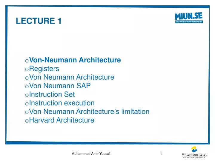
Lecture 1. Von-Neumann Architecture Registers Von Neumann Architecture Von Neumann SAP Instruction Set Instruction execution Von Neumann Architecture’s limitation Harvard Architecture. The Basic Register.

E N D
Lecture 1 • Von-Neumann Architecture • Registers • Von Neumann Architecture • Von Neumann SAP • Instruction Set • Instruction execution • Von Neumann Architecture’s limitation • Harvard Architecture Muhammad Amir Yousaf
The Basic Register • A register is a storage device that is capable of holding the collection of one or more bits. 0 1 . . n-1 D0 Dn-1 Clk N bit Register R,/W En D0 Dn-1 Muhammad Amir Yousaf
Data Transfer between registers 1 1 0 1 Control Signal R1, /W1 Clk 0 0 1 1 . . . . n-1 n-1 D0 Dn-1 En1 Clk D0 Dn-1 R2,/W2 En2 Muhammad Amir Yousaf
CPU Both data and instructions at the same system bus System bus Memory Executionunit MAR VON Neumann architecture Register A ALU Register B PC IR Output Register Controller Control unit Binary Display Muhammad Amir Yousaf
Ea Register A Lm MAR La Clk VON Neumann SAP ALU S RAM 16 x 8 E Lb Register B CPU CE Clk PC clr PC Ep Lo Cp Output Register IR clr Li Ei Clk Controller Binary Display clr Simple As Possible Computer EpCpEiLiEaLaS E LbLmCE Lo Muhammad Amir Yousaf
Components in a microprocessor system Instruction set • The instruction set specifies the basic operations supported by the machine. • It provides an interface to the underlying hardware. • It expresses the machine’s ability to transfer data, store data, operate on data and make decisions. • Arithmetic and Logic Instruction. • Looping and decision making. • Transfer of data. • Transfer of control. Muhammad Amir Yousaf
Components in a microprocessor system Instruction set • The entities that instructions operate on are denoted operands. • The number of operands that an instruction operate on is called arity of operation. ADD 9H ADD R1,R2 z = x+y; x = x+y; x++; Muhammad Amir Yousaf
More on Instructions Operand 0 Source Operand 1 Src / Destination Operand 0 (Source and/or Destination) Operation Operation Operation Operand 2 Src / Dest Operand 1 Src Operand 0 Src 15 15 15 x x x 0 0 0 • The size of operation field is determined by the number of instructions a machine supports. • Each instruction is given a unique code called op-code Muhammad Amir Yousaf
Components in a microprocessor system Instruction set for SAP Instruction Operation 000 Load RAM data into Register A 001 Add RAM data to RegisterA 010 Subtract RAM data from RegisterA 011 Load RegisterA into Output register 111 Stop Processing Muhammad Amir Yousaf
Components in a microprocessor system • These numbers, called op-codes can be stored in program memory and can be fetched by the computer during execution. • Mnemonic names are given to op-code’s binary pattern to make them easier to work with. Instruction set Mnemonics Op-codes Operation LDA 0000 Load RAM data into Register A ADD 0001 Add RAM data to RegisterA SUB 0010 Subtract RAM data from RegisterA OUT 0011 Load RegisterA into Output register HLT 1111 Stop Processing • Assembler translate these mnemonics to op-codes Muhammad Amir Yousaf
Components in a microprocessor system • LDA instruction includes the hex address of the data to be loaded. • LDA 8H • ADD instruction includes the address of the word to be added into RegisterA. • ADD 9H means ‘add the contents of memory location 9H to the RegisterA’; the sum replaces the original contents of RegisterA • SUB instruction includes the address of the word to be subtracted. • RegisterB holds the word to be operated, adder/sub compute instantly and the result is written on RegisterA. Instruction set Muhammad Amir Yousaf
Components in a microprocessor system Programming sap 0H : 0000 1001 How instructions are stored in the memory? Assembly language: language of mnemonics Machine language : language of 1,0 strings Muhammad Amir Yousaf
Ea Register A Lm MAR La Clk Addresses • Each location in memory has an associated address. • Information is accessed in memory by giving that. • If a memory has 16 locations, it will have 16 addresses. • Address word size to access all the locations? ALU S RAM 16 x 8 E Lb Register B CPU CE Clk PC clr PC Ep Lo Cp Output Register IR clr Li Ei Clk MSB N-1 Big Endian 0 Controller Binary Display clr Little Endian MSB N-1 0 EpCpEiLiEaLaS E LbLmCE Lo Muhammad Amir Yousaf
Ea Register A 0 000 Lm La 0 000 0 000 Clk MAR Instruction execution cycle ALU S E RAM 16x8 Lb Register B 0 000 CPU CE Clk PC clr 0 000 PC Ep Lo Cp Output Register 0 000 IR clr 0 000 Li Ei Clk Controller Binary Display clr PC MAR EpCpEiLiEaLaS E LbLmCE Lo Fetch instr. Muhammad Amir Yousaf
Instruction Execution Cycle Ea Register A Lm 0 000 La Clk MAR ALU S E RAM 16x8 Lb Register B CPU CE Clk PC clr 0 000 0 00 1 PC Ep Lo Cp Output Register IR clr Li Ei Clk Controller Binary Display clr PC Inc EpCpEiLiEaLaS E LbLmCE Lo Fetch instr. Muhammad Amir Yousaf
Instruction Execution Cycle Ea Register A Lm 0 000 0000 1001 La Clk MAR ALU S 0H:00001001 E 0H: xxxxxxx Lb Register B 0000 1001 RAM 16x8 CPU CE Clk PC clr 0 00 1 PC Ep Lo Cp Output Register 0000 1001 clr 00001001 0000 1001 Li Ei IR Clk Controller Binary Display clr Mem IR EpCpEiLiEaLaS E LbLmCE Lo Fetch instr. Muhammad Amir Yousaf
Instruction Execution Cycle Ea Register A Lm 0 000 1 0 0 1 1001 La Clk MAR ALU S 0H:0101001 E 1H: xxxxxxx Lb Register B 1001 RAM 16x8 9H: 00000001 CPU CE Clk PC clr 0 00 1 PC Ep Lo Cp Output Register 1001 clr 1001 0000 1001 Li Ei IR Clk Controller 1001 Binary Display clr EpCpEiLiEaLaS E LbLmCE Lo Fetch instr. Decode instr. Muhammad Amir Yousaf
Instruction Execution Cycle Register A Ea 00000001 Lm 1 0 0 1 00000001 La Clk MAR ALU S 0H:0101001 E 1H: xxxxxxx Lb Register B 00000001 RAM 16x8 9H: 00000001 CPU CE Clk 0 000000 1 PC clr 0 00 1 PC Ep Lo Cp Output Register 00000001 clr 1001 0000 00000001 Li Ei IR Clk Controller Binary Display clr EpCpEiLiEaLaS E LbLmCE Lo Fetch instr. Decode instr. Fetch operand Muhammad Amir Yousaf
Instruction Execution Cycle Register A Ea 00000001 Lm 1 0 0 1 00000001 La Clk MAR ALU S 0H:0101001 E 1H: xxxxxxx Lb Register B 00000001 RAM 16x8 9H: 00000001 CPU CE Clk 0 000000 1 PC clr 0 00 1 PC Ep Lo Cp Output Register 00000001 clr 1001 0000 00000001 Li Ei IR Clk Controller Binary Display clr EpCpEiLiEaLaS E LbLmCE Lo Fetch instr. Decode instr. Fetch operand Execute Write result Muhammad Amir Yousaf
Responsible for moving data around inside the processor . • Bringing data in from outside and sending data out. • Each data transfer instruction has three pieces of information: • The data • The source • The destination. • The source and destination can be: • A register • Memory • IO port • The path to actual selection of operands is controlled by ‘addressing mode’ specified by operand. Data Transfer Instructions Muhammad Amir Yousaf
A portion of each operand field is designated as specification to the hardware as how to interprete the information in the remaining bits of operand fields. • A microprocessor design implements four to eight addressing modes. • Common addressing modes are: • Immediate • Direct and Indirect • Register Direct and Register Indirect • Indexed • Program counter Relative. Data Transfer Instructions Muhammad Amir Yousaf
Direct and Indirect • Common addressing modes are: Data Transfer Instructions • Immediate • Register Direct and Register Indirect Muhammad Amir Yousaf
Common addressing modes are: Data Transfer Instructions • Indexed • Program counter Relative Muhammad Amir Yousaf
Von Neumann Limitation • The shared bus between the program memory and data memory leads to the Von Neumann bottleneck. • Because program memory and data memory cannot be accessed at the same time, throughput is much smaller than the rate at which the CPU can work. • The CPU is continuously forced to wait for needed data to be transferred to or from memory. • For example if we try to read an operand at the same time as we try to read an instruction. This is not possible in the von Neumann architecture since we only have one system bus and cannot address two memory positions simultaneously. Muhammad Amir Yousaf
Other Architectures Harvard Architecture • In the Harvard architecture this is solved by having two separate system buses: • One for instructions • One for data • Data and instructions can be loaded simultaneously, which improves the efficiency. • Means more I/O signals. • More expensive processor. • Uses more power. • Is used internally in modern 32-bit microprocessors and RISC processors. Program Memory Program system Bus CPU Computer Memory IOs Data system Bus Muhammad Amir Yousaf
microprocessor System design General Purpose Computer e.g PC A general-purpose computer, such as a personal computer (PC), is designed to be flexible and to meet a wide range of end-user needs. Embedded Systems An embedded system is designed and optimized to perform a specific task very efficiently. • They are different in: • Resources • Real time. • Robustness • Outer world interaction (IOs) • Program structure Muhammad Amir Yousaf
microprocessor System design Embedded Systems An embedded system is designed and optimized to perform a specific task very efficiently. Microprocessor based systems: A microprocessor is an integrated implementation of central processing unit portion (CPU). Use separate integrated circuits for memory and peripherals. Muhammad Amir Yousaf
microprocessor System design Embedded Systems An embedded system is designed and optimized to perform a specific task very efficiently. Microcontroller based systems: A microcontroller brings together a microprocessor core and a rich collection of peripherals and IO capability into single integrated circuit. Reduces cost and size. Timers, ADC, DAC, DIO, serial and parallel communication channels, DMA Muhammad Amir Yousaf
Instruction addressing modes Instruction Architecture Operand1 Operand2 Opcode 0 3 4 15 Instruction: Add with register Opcode : 0011 or 3 Operand : address of memory location, register or constant RISC vs CISC Addressing modes Muhammad Amir Yousaf
Components in a microprocessor system • CISC (Complex Instruction Set Computer) • The primary goal of CISC architecture is to complete a task in as few lines of assembly as possible. • This is achieved by building processor hardware that is capable of understanding and executing a series of operations. • "MULT“. When executed, this instruction loads the two values into separate registers, multiplies the operands in the execution unit, and then stores the product in the appropriate register. Thus, the entire task of multiplying two numbers can be completed with one instruction: • MULT 2:3, 5:2 Processor Types: Muhammad Amir Yousaf
Components in a microprocessor system Reduced instruction set computing • RISC (Reduced Instruction Set Computer) • RISC processors only use simple instructions that can be executed within one clock cycle. • Thus, the "MULT" command described above could be divided into three separate commands: • LOAD, which moves data from the memory bank to a register, • PROD, which finds the product of two operands located within the registers. • STORE, which moves data from a register to the memory banks. • A programmer would need to code four lines of assembly: • LOAD A, 2:3LOAD B, 5:2PROD A, BSTORE 2:3, A Muhammad Amir Yousaf
Components in a microprocessor system Memory: • To store data or instructions the computer system uses a so-called primary memory • The executable program code and data is stored in main memory. • The primary memory is divided in two main parts • RAM • ROM The memory can be seen as a number of post boxes Muhammad Amir Yousaf
Primary Memory RAM CPU ROM I/O unit The outer world/ The user Von Neumann Architecture Microcontrollers • What does a computer system comprise: • Processor (CPU, Central Processing Unit) • Memory • Peripheral units, I/O • System bus, to communicate with peripheral units • If we have a chip that comprise all this it is often called a ‘Micro Controller’ Muhammad Amir Yousaf
Components in a microprocessor system • Data bus • Communication channel to move data to and from CPU and peripheral units. • Address bus • Used to point out which memory position or IO port that is to be read or written. Processor system bus • Control signals • Used to signal when a data transaction starts and stops. • For example signals if a transaction is a read or write operation. Muhammad Amir Yousaf
References • Lecture slides: Benny Thörnberg, Mattias O’ Nils • Video Lecture: Prof. Anshul Kumar • http://www.computersciencelab.com/ComputerHistory/History.htm • Webopedia • http://www.world-war-2-planes.com/american-world-war-2-planes.html (slide 12) • http://www.anvari.org/cols/Typewritter_ASCII_Art/Steam_Engine_Number_3.html (slide 10) • http://www.old-computers.com/history/detail.asp?n=61 (slide 15) • http://www.freewebs.com/computingstudies/S1_UT_Systems/S1UTSystems_07.htm • http://www.computer-museum.org/index.html • http://www.ucdsb.on.ca/school/sla/aboutus/Pages/ExamSchedule.aspx • http://www.youtube.com/watch?v=AqbyMRs3ocs • Camera Pills Use MEMS Micro Reed Sensors to Activate the Battery • http://en.wikipedia.org/wiki • http://www-cs-faculty.stanford.edu/~eroberts/courses/soco/projects/risc/risccisc/ Muhammad Amir Yousaf