Download
1 / 31
310 likes | 492 Views
Separable 2D Convolution with Polymorphic Register Files . C ă t ă lin Ciobanu Georgi Gaydadjiev Computer Engineering Laboratory Delft University of Technology The Netherlands and Department of Computer Science and Engineering Chalmers University of Technology Sweden.

E N D
Separable 2D Convolution with Polymorphic Register Files CătălinCiobanu GeorgiGaydadjiev Computer Engineering Laboratory Delft University of Technology The Netherlands and Department of Computer Science and Engineering Chalmers University of Technology Sweden
SIMD register files evolution IBM Cell BE, 2005 Cell SPU: 128 registers, 128 bits each Cell PPU Altivec: 32 registers, 128 bits each Earth Simulator 2 (ES2), 2009 NEC SX-9/E/1280M160 (ranked 145 in Top 500, June 2012) Vector Unit: 72 registers, 256 elements each Intel Sandy Bridge, 2011 Advanced Vector Extensions (AVX) 16 registers, 256 bits each
Choosing the parameters of the SIMD RF • Design time: number of registers, their shape/sizes • Programmers are expected to optimize the code accordingly • Next generation designs “may” break software compatibility • Software is able mask low level architectural details • In domains with efficiency constraints (e.g, HPC), hardware support is preferable • Offering a single golden configuration is often impossible as new workloads will emerge for sure
Polymorphic Register File architecture • Purpose: • Adapt to data structures; • Reduced number of opcodes, richer instructions semantics; • Focus on functionality, not on complex data operations / transfers. • Advantages: • Simplified vectorization, 1-to-1 mapping of registers and data; • Changing the register number / sizes respects compatibility; • Improved storage efficiency; • Potential performance gains; • Reduced binary code sizes. Example PRF, 14x8 storage size A logical register: Base, Horizontal and Vertical Length, Data Type & Width Example: Mx× row vector vmul R9,R1,R2
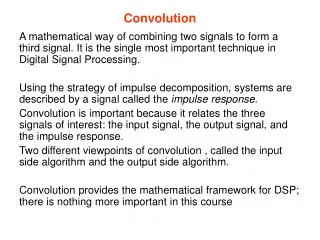
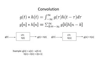
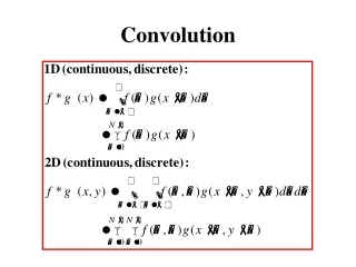
Convolution Used for signal filtering • digital signal processing • image processing • video processing • … Examples: • Gaussian blur filters • reduce the image noise and detail • Sobeloperator • edge detection algorithms
Convolution (continued) • A “blending” between the input and the mask • Each output is a weighted sum of its neighbors • A mask defines the products coefficients • used for all elements of the input array • No data dependencies • very suitable for SIMD implementations
1D Convolution example • Special case for border elements • Apply mask to elements outside the input • Assumptions required for these ”halo” elements • For example: consider all halo elements to be 0
Separable 2D Convolution • computed as two 1D convolutions • row-wise 1D followed by column-wise 1D convolution • Fewer operations are required • More suitable for blocked SIMD execution • fewer data dependencies between blocks
Our Implementation Separable 2D Convolution • Execute two consecutive 1D convolutions • Transpose the data while processing • We only present the first 1D convolution step • Should be executed twice
Conflict-free Transposition • Column-wise Convolution involves stridedaccesses • may degrade performance due to bank conflicts Solution: • Vectorized transpositionwhile processing data • transpose the output of 1st 1D convolution • Conflict-free using Polymorphic RFs • Avoids strided accesses for 2nd 1D convolution
Conflict-free Transposition • R 6 - 9 • loaded using 1D accesses • R 10 – 13 • stored using 1D accesses • Result effectively transposed • Full LS bandwidth utilization • only consecutive addresses
Vectorized Separable 2D Convolution • We separate the algorithm in three parts • first (left-most) • main (middle) • last (right-most) • 2D vectorization • Data is be processed multiple rows at a time • Our examples: blocks with 4 rows, 6 columns
Three Separate Convolution Phases Main Customize the PRF • Runtime customization • Only logic registers resizing • Instructions not modified First Last
Register Assignments • R1: input data • Overlaps with R6-R9 • R2: the mask • R3: convolution result • Overlaps with R10-R17 • R0: left hallo cells • R4: halo + loaded data • R5: right halo for next block
Throughput Comparison – NVIDIA C2050 NVIDIA Tesla C2050 GPU • State of the art Fermi architecture • 448 SIMD lanes running at 1.15 GHz • 14 Streaming Multiprocessors, 32 SIMD lanes each • 3GB off-chip GDDR5 @ 1.5GHz • 384-bit wide,144GB/s • Power consumption of 247 Watts • 64KB L1 cache, 768KB unified L2 cache
Throughput Comparison – PRF Polymorphic Register File (PRF) • Same clock frequency as the C2050 GPU assumed • Realistic based on our ASIC synthesis results • Up to 256 SIMD lanes • Private Local Store (LS), 11 cycles latency • Multiple LS bandwidth scenarios • 16 bytes / Cycle (the same as Cell SPU) up to 256 bytes /cycle • Blocked Separable 2D convolution implementation • 32 x 32 elements block size
Constrained Local Store BW: 16 B / cycle Saturates for > 4 lanes Outperform GPU
Local Store BW: 32B/cycle 8 lanes match GPU throughput
Local Store BW: 64B / Cycle 2X than for 16B/Cycle 4 lanes match GPU throughput
Local Store BW: 128 B / Cycle Improvement mostly for > 32 lanes
SIMD lanes and LS BW Efficiency Summary SIMD lanes range providing at least 75% efficiency • If PRF implemented in FPGA technology • Dynamically adjust #vector lanes during runtime • Switch off unused lanes to save power • Customize LS BW for high performance or power savings
Conclusions • PRFs outperform the NVIDIA Tesla GPU for 2D Convolution with masks of 9 × 9 or larger • even in bandwidth constrained systems • Large mask sizes allow the efficient use of more PRF vector lanes • For small mask sizes, LS bandwidth is the main bottleneck • PRFs reduced the effort required to vectorize each Convolution execution phase • Simplified to resizing the PRF registers on demand
Unified assembly vector instructions Unified opcodes: multiplication • Matrix x Vector vmul R3, R0, R2 • Vector x Vector (main diag.) vmul R5, R1, R4 • Integer / Floating point 8/16/32/64-bit The micro-architecture will perform the compatibility checks and raise exceptions
The bandwidth utilization problem Poor memory bandwidth utilization ReOscheme Optimal
ASIC PRF implementation overview • TSMC 90nm technology • Synthesis tool: Synopsys Design Compiler Ultra F-2011.09-SP3 • Artisan memory compiler (1GHz, 256x64-bit dualportSRAM as storage element) • 64 bit data width • Full crossbars as read and write shuffle blocks • 2R/1W ports • Four multi-lane configurations • 8 / 16 / 32 / 64 lanes • Three PRF sizes: • 32KB (64x64), 128KB (128x128), 512KB (256x256) • Clock frequency: 500 MHz - 970MHz • Dynamic Power: 300mW – 8.7W • Leakage: 10mW – 276mW • Customized configurations • Up to 21% higher clock frequency • Up to 39% combinational hardware area reduction • Up to 10% reduction in total area • Reduced dynamic power by up to 31%, leakage with nearly 24%
Customized linear addressing functions The PRF contains data elements, supporting up to parallel vector lanes It is possible to determine the linear address by only examining the upper left corner of the block being accessed for each memory module (k, l): • and coefficients: • depend on the MAFs and shape/size of the accesses, being are different for each of the selected schemes • The inverse MAF is required:
Multi-view parallel access schemes • Conflict-free parallel access for at least two rectangular shapes • Relaxes the p × q rectangle limitation of the ReO scheme
Implementation diagram • Data is distributed among p x q memory modules • The AGU computes the addresses of all involved elements • The generated addresses are fed to the Module Assignment Function (MAF), which controls the read and write shuffles • Standard case: addresses need to be reordered according to the MAF before being sent to the memory modules • Customized case: eliminate the need to shuffle the read and write intra-module addresses. • The shaded blocks are replaced by the ci, cj coefficients as well as the customized addressing function