Download
1 / 18
190 likes | 470 Views
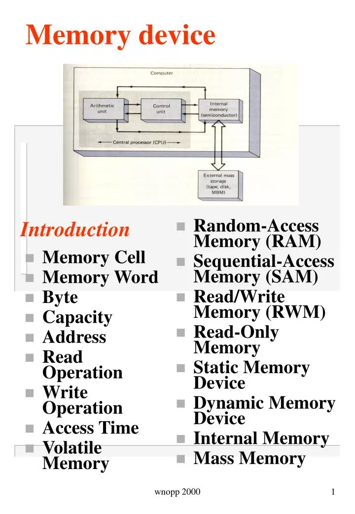
Memory device. Introduction. Random-Access Memory (RAM) Sequential-Access Memory (SAM) Read/Write Memory (RWM) Read-Only Memory Static Memory Device Dynamic Memory Device Internal Memory Mass Memory. Memory Cell Memory Word Byte Capacity Address Read Operation Write Operation

E N D
Memorydevice Introduction • Random-Access Memory (RAM) • Sequential-Access Memory (SAM) • Read/Write Memory (RWM) • Read-Only Memory • Static Memory Device • Dynamic Memory Device • Internal Memory • Mass Memory • Memory Cell • Memory Word • Byte • Capacity • Address • Read Operation • Write Operation • Access Time • Volatile Memory wnopp 2000
General Memory Operation • Select the address. • Select R/W operation. • Supply the input to be store (W operation). • Hold the output data comings from memory (R operation). • Enable (or Disable) the memory Example Memory chip 2K x 8. How many total bits can chip store? 2K = 1 x 1024 = 2048 words 1 word = 8 bits 2K x 8 = 2048 x 8 = 16384 bits Which memory store the most bits: 5M x 8, 1M x 16 5M x 8 = 5 x 1,048,576 x 8 = 4,1943,040 bits 1M x 16 = 1,048,576 x 16 = 1,677,7216 bits wnopp 2000
CPU- Memory connections Write operation 1. CPU ๐Binary address on address bus. 2. CPU ๐Data on data bus. 3. CPU ๐control signal. 4. ICs decode address location. 5. Transfer data to the selected location. Read operation 1. CPU ๐Binary address on address bus. 2. CPU ๐control signal. 3. ICs decode address location. 4. Place data ๐ data bus ๐ Transfer data to CPU wnopp 2000
Read-Only Memory wnopp 2000
ROM architecture wnopp 2000
ROM timing read operation PROMs fusible links wnopp 2000
Example of a programmable logic device wnopp 2000
PROM architecture for PLDs wnopp 2000
PAL architecture wnopp 2000
Symbol & mode table for 6264 SRAM Cell arangement in 16Kx1 DRAM Symbolic representation of DRAM wnopp 2000