Download

1 / 45
450 likes | 604 Views
This presentation provides an overview of datapath design and control signals in processor design. It covers basic functional units, instruction sequencing, operations on data in registers, and memory. The content includes single-cycle and multicycle implementation schemes with relevant diagrams and tables.

E N D
Processor Design Datapath and Design
All tables and diagrams in this presentation are from: D. Patterson and J. Hennessy, Computer Organization and Design: The Hardware/Software Interface, Third Edition (The Morgan Kaufmann Series in Computer Architecture and Design), Morgan Kaufmann, 2002.
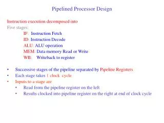
Simple Implementation Scheme Single cycle Implementation
Intstruction fetch IR <= Memory[PC]; PC <= PC+4 IR <= Memory[PC]; PC <= PC+4
IorD= 0 MemRead= 1 IRWrite= 1 IR <= Memory[PC];
PCSource= 01 PCWrite= 1 ALUOp= 00 ALUSrcB= 01 ALUSrcA= 0 PC <= PC+4
Intstruction decode/register fetch A <= Reg[ IR [25:21]]; B <= Reg[ IR [20:16] ]; ALUOut <= PC + ( SignExt( IR[15:0] ) << 2 ) A <= Reg[ IR [25:21]]; B <= Reg[ IR [20:16] ]; ALUOut <= PC + ( SignExt( IR[15:0] ) << 2 )
ALUOp = 00 ALUSrcB = 11 ALUSrcA = 0 ALUOut <= PC + ( SignExt( IR[15:0] ) << 2 )
R-type instruction ALUOut <= A op B Reg[ IR[15:11] ] <= ALUOut ALUOut <= A op B Reg[ IR[15:11] ] <= ALUOut
ALUOp = ?? ALUSrcB = 0 ALUSrcA = 1 ALUOut <= A op B
RegWrite = 1 MemtoReg = 0 RegDst = 1 Reg[ IR[15:11] ] <= ALUOut
Load instruction ALUOut <= A + SignExt(IR[15:0]) MDR <= Memory[ALUOUT] Reg[IR[20:16] ] <= MDR ALUOut <= A + SignExt(IR[15:0]) MDR <= Memory[ALUOUT] Reg[IR[20:16] ] <= MDR
ALUOp = 00 ALUSrcB = 10 ALUSrcA = 1 ALUOut <= A + SignExt(IR[15:0])
IorD =1 MemRead =1 RegWrite =1 MemtoReg =1 RegDst = 0 MDR <= Memory[ALUOUT] ; Reg[IR[20:16] ] <= MDR