Download
1 / 64
680 likes | 889 Views
some things you might be interested in knowing about Graphene. height. length. width. All Natural Object/Materials Are 3D. quasi-2D. 3D. quasi-1D. quasi-0D. NO Bottom-Up Approach. 400 carbon atoms at 2000 K. growth means temperature means violent vibrations in 2D.

E N D
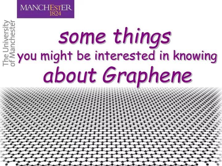
some things you might be interested in knowingabout Graphene
height length width All Natural Object/Materials Are 3D quasi-2D 3D quasi-1D quasi-0D
NO Bottom-Up Approach 400 carbon atoms at 2000 K growth means temperature means violent vibrations in 2D Fasolino (Nijmegen) growth of macroscopic 2D objects is strictly forbidden Peierls; Landau; Mermin-Wagner; … (only nm-scale flat crystals possible to grow in isolation)
No Bottom-Up for 2D Crystals largest known flat hydrocarbon: 222atoms/37rings (Klaus Müllen 2002) graphene: least stable configuration for <24,000 atoms (Don Brenner 2002) above this number (~20 nm), scrolls are most stable
ONE-ATOM-THICK OBJECTS, HUGE MACRO-MACROMOLECULES? (not only graphene)
Top-Down Approach? just extract one atomic plane from a bulk crystal
isolating individual atomic planes starting point in <<2004 suggested in print Nature Mater 2007 epitaxial growth MANY MANY DIFFERENT EPITAXIAL SYSTEMS including graphitic layers Grant 1970 (on Ru) Bommel 1975 (SiC) McConville 1986 (on Ni) Land 1992 (on Pt) Nagashima 1993 (on TiC) Forbeaux 1998 (SiC) de Heer 2004 (SiC) … … let us remove the substrate chemically, like SiN or C membranes monolayer is a part of the 3D crystal GOAL: NOT EPITAXIAL LAYERS but rather ISOLATED ATOMIC PLANES
Poor Man Approach 3D LAYERED MATERIAL extract individual atomic planes
start with graphite need strong in-plane bonds Also: Kurtz 1990; Ebbesen 1995; Ohashi 1997 Ruoff 1999; Kim 2005; McEuen 2005 split into increasingly thinner “pancakes” one atomic plane deposited on Si wafer SEM: down to ~30-100 layers 1 mm until we found a single layer called GRAPHENE Manchester, Science 2004; PNAS 2005
extracting atomic planes en masse SPLIT INTO ATOMIC PLANES ANY LAYERED MATERIAL WHEN YOU KNOW THAT ISOLATED ATOMIC PLANES CAN EXIST
Splitting Graphite into Graphene 15 min centrifugation 100nm TEM few hours sonication in organic solvent (chloroform, DMF, etc) Manchester, Nanolett ’08 Coleman et al, Nature Nano ’08 relevant literature: INTERCALATED GRAPHITE TEM observations of ultra-thin graphite from Ruess 1948 to Boehm 1962 to Horiuchi 2004 graphene oxide paper Brodie 1859 Kohlschutter 1918 RENAISSANCE starting with graphene oxide: Ruoff, Nature 2006 also, Kern’s, Kaner’s groups
Kong ‘09 CHEMICAL EXTRACTION chemically extract epitaxially grown atomic planes S. Seo (Samsung 2010) chemically remove the substrate FIRST DEMONSTRATED Kong et al, Nanolett 2009 on Ni Hong, Ahn et al, Nature 2009 on Ni Ruoff et al, Science 2009 on Cu as suggested, Nature Mat 2007 graphene-on-Si wafers uniform; no multilayer regions; some cracks; >5,000 cm2/Vs
EXTRACTION ONTO SAME SUBSTRATE atomic planes decouple during cooling and/or intercalated Mallet et al 2007 RELATIVELY WEAK INTERACTION WITH THE GROWTH SUBSTRATE de Heer2004; Rotenberg 2006; Seyller 2008 special case: SiC as an insulator DECOUPLED FURTHER BY PASSIVATION Starke 2010; Yakimova 2010
Many Other 2D Materials Possible 2D NbSe2 in AFM 0Å 8Å 23Å 50 m 1m 1 m 1 m 2D Bi2Sr2CaCu2Ox in SEM 2D MoS2 in optics 2D boron nitride in AFM also, 2,3,4… layers NOT ONLY NATURALLY LAYERED MATERIALS! THINK OF EPITAXY! Manchester, PNAS ’05
MESSAGE TO TAKE AWAY MATERIALS OF A NEW KIND: ONE ATOM THICK atomic planes of graphite and other materials were KNOWN before as constituents of 3D systems now we can ISOLATE, STUDY and USE them - and importantly - they are worth of!
what is so special about graphene?
GRAPHENE’S SUPERLATIVES thinnest imaginable material largest surface-to-weight ratio (~2,700 m2 per gram) strongest material ‘ever measured’ stiffest known material(stiffer than diamond) most stretchable crystal (up to 20% elastically) record thermal conductivity (outperforming diamond) highest current density at room T (106 times of copper) highest intrinsic mobility (100 times more than in Si) conducts electricity in the limit of no electrons lightest charge carriers (zero rest mass) longest mean free path at room T (micron range) completely impermeable (even He atoms cannot squeeze through)
EXCEPTIONAL ELECTRONIC QUALITY & TUNABILITY
SiO2 Si graphene 6 4 resistivity(k) 2 0 -100 -50 0 50 100 gate voltage(V) AMBIPOLAR ELECTRIC FIELD EFFECT Manchester, Science 2004 • CONTROL ELECTRONIC PROPERTIES homogenous electric doping from ~108 to ~1014 cm-2 • ASTONISHING ELECTRONIC QUALITY ballistic transport on submicron scale under ambient conditions holes ~1013 cm-2 electrons ~1013 cm-2 weak e-ph scattering POSSIBLE ROOM-T MOBILITY above 200,000 cm2/V·s Manchester, PRL 2008 Fuhrer’s group, Nature Nano 2008 carrier mobility at 300K routinely: ~15,000 cm2/V·s
10 um 6 graphene Hall bar BN 2 0 Si wafer 1 3 CURRENT STATUS graphene on atomically flat boron nitride room-T mobility > 50,000 cm2/V·s also, Columbia group, arxiv 2010
2 m 2 K CURRENT STATUS suspended graphene 2-terminal suspended devices: first reported by Andrei, Kim & Yacoby low-T mobilities few million cm2/V·s SdH oscillations start ~50G level degeneracy lifted ~ 500G Manchester, unpublished
UNIQUE ELECTRONIC STRUCTURE Wallace 1947
massive chiral fermions massless Dirac fermions monolayer graphene bilayer graphene McClure 1958 McCann & Falko 2006
Finding Electronic Structure B (T) 140K 0 4 8 12 1 6 12T 0.6 10K 80K xx (k) xx (1/k) Vg = -60V 0 20K 0.4 4 0 25 50 75 100 n =4B/φ0 Vg (V) 8T 2 4K 1 xx(k) ωcτ=const +10V (a.u.) 0 -100 -50 0 50 100 +90V 0 0 150 T (K) Vg (V) Manchester, Science ’04 & Nature ‘05 degeneracy f =4 two spins & two valleys
Finding Electronic Structure E=pvF 0.06 mc/m0 0.04 S ky 0.02 kx 0 -6 -3 0 3 6 n (1012 cm-2) ZERO REST MASS: effective mass E= mcvF2 BF =(ħ/2πe)S andmc =(ħ2/2π)∂S/∂E experimental dependences BF ~ nand mc ~ n1/2 necessitates S ~ E(k)2 or E ~k vF= 1.0·106 m/s 5% mass of charge carriers strongly depends on concentration in agreement with theory: Wallace 1947, McClure 1958, Semenoff 1984
massive & massless Dirac fermions xx (k) xx (k) xy (4e2/h) xy (4e2/h) 4 12T 3.5 12T 3 2 2.5 4K 1 10 1.5 0 -1 0.5 -2 -0.5 -3 5 -4 -1.5 -2.5 -3.5 6 0 n (1012 cm-2) n (1012 cm-2) 4 -4 -2 0 2 4 2 0 -4 -2 0 2 4 half-integer QHE relativistic analogue of integer QHE “anomalous” QHE Manchester, Nature ’05; Columbia, Nature ’05 Manchester+Lancaster, Nature Phys ’06
robust quantum Hall phenomena 0.6 B =16 T 250K 30T 4 30 200K 2 150K quantum capacitance xx(k) 20 0 xy (e2/h) 300K 100K -2 0.4 30K 10 -4 -6 -1 0 1 0 gate voltage (V) -60 -30 0 30 60 gate voltage (V) zero LL directly in the density of states room-temperature QHE Manchester+Columbia, Science ‘07 Manchester, PRL 2010
NEW PHYSICS ACCESS TO RELATIVISTIC-LIKE PHYSICS IN CONDENSED MATTER EXPERIMENT
EXAMPLE #1: Klein Tunnelling
Klein Tunnelling Klein 1929 Katsnelson + Manchester 2006 Falko et al 2006 Gorbachev et al, Nanolett ’08 Stander et al, PRL ’09 Young et al, Nature Phys ‘09
EXAMPLE #2: conductivity “without” charge carriers Manchester, Nature ’05
Minimum Quantum Conductivity ρmax 10K 6 E =0 4 ρ(k) 2 0 -80 -40 0 40 80 zero-gap semiconductor Vg (V) no localization in the peak down to 30mK and for million-range mobilities
Minimum Quantum Conductivity data from 2007 annealing 2 min(4e2/h) recent samples with million mobility 1 1/ 0 0 4,000 8,000 12,000 (cm2/Vs) “quantized” conductivity NOT conductance (~e2/h per spin and valley) one electron per sample makes it a metal Fradkin 1986; Lee 1993; Ludwig 1994; Morita 1997; Ziegler 1998 … Peres 2005; Gusynin 2005; Katsnelson 2006; Tworzydlo 2006; Cserti 2006; Ostrovsky 2006 …
Minimum “Mott” Conductivity Mott’s argument: not the case of other materials NO LOCALIZATION AG & Allan MacDonald, Phys. Today 2007
EXAMPLE #3: visualization of fine structure constant Manchester, Science 2008
graphene 100 µm bilayer air 100 98 white light transmittance (%) 96 0 25 50 distance (m) GRAPHENE OPTICS Manchester, Science ’08 one-atom-thick single crystal visible by naked eye
graphene e2 c = bilayer (nm) air 500 600 700 1.5 100 1.0 G (e2/2h) 98 white light transmittance (%) 0.5 96 0 25 50 distance (m) GRAPHENE OPTICS 100 2.3% light transmittance (%) 90 theory of 2D Dirac fermions: Gusynin ‘06 Kuzmenko ‘08 80 1.5 2.0 2.5 3.0 E (eV) coupling of light with relativistic-like charges should be described by coupling constant a.k.a. fine structure constant one-atom-thick single crystal visible by naked eye
EXAMPLE #4: relativistic fall on superheavy nuclei Shytov et al PRL 2007 Castro Neto et al PRL 2007 …..
Atomic Physics Z supercritical regime Z Positron emission slides courtesy of Antonio Castro Neto
Graphene Physics “artificial atoms” easily become overcritical Z
EXAMPLE #5: New Graphene-Based Materials Manchester, Science ’09 & arxiv 2010
Graphene as GigaMolecule GRAPHENE both surfaces available (bi-surface chemistry; chemistry of individual gigamolecules) chemical reactions: C + X => CX
FluoroGraphene make large graphene membranes expose them from BOTH side to atomic F (using XeF2) Raman, optics, TEM, XPS, transport
fluorographene 30h 6 20h 9h 4 intensity (a.u.) 1h 2D 2 G pristine D 0 1200 1600 2600 3000 Raman shift(cm-1) FluoroGraphene make large graphene membranes expose them from BOTH side to atomic F (using XeF2) CHANGES IN RAMAN XPS & EDX: C:F 1 Raman, optics, TEM, XPS, transport
Stoichiometric Derivative fluorographene (“2D Teflon”) optical gap of 3.0eV chemical reactions: C + F => (CF) wide-gap semiconductor chemically & thermally stable mechanically strong exposure to atomic fluorine, using XeF2
MESSAGE TO TAKE AWAY CORNUCOPIA OF NEW SCIENCE not only electronic properties but optical, mechanical, chemical, etc.
WHAT ABOUT APPLICATIONS? INDUSTRIAL SCALE PRODUCTION IS A DONE DEAL
APPLICATION OVERVIEW only realistic examples
EXAMPLE #1: ON SALE ALREADY