Download
1 / 17
180 likes | 369 Views
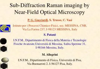
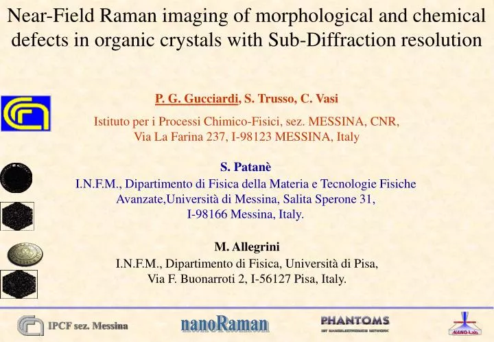
Near-Field Raman imaging of morphological and chemical defects in organic crystals with Sub-Diffraction resolution. P. G. Gucciardi , S. Trusso, C. Vasi Istituto per i Processi Chimico-Fisici, sez. MESSINA, CNR, Via La Farina 237, I-98123 MESSINA, Italy. S. Patanè

E N D
Near-Field Raman imaging of morphological and chemical defects in organic crystals with Sub-Diffraction resolution P. G. Gucciardi, S. Trusso, C. Vasi Istituto per i Processi Chimico-Fisici, sez. MESSINA, CNR, Via La Farina 237, I-98123 MESSINA, Italy S. Patanè I.N.F.M., Dipartimento di Fisica della Materia e Tecnologie Fisiche Avanzate,Università di Messina, Salita Sperone 31, I-98166 Messina, Italy. M. Allegrini I.N.F.M., Dipartimento di Fisica, Università di Pisa, Via F. Buonarroti 2, I-56127 Pisa, Italy.
Outline Motivations: Difficulties: • Chemical Imaging. • Stress Imaging. • High spatial resolution: 100 nm. • Added value: simultaneous sample topography and elastic scattering images. • Low efficiency of the Raman scattering. • Low throughput of the SNOM Fiber probes. • Very long acquisition times for Imaging purposes. • High mechanical and thermal stability are required. • Investigated Samples: • Tetracyanoquinodimethane (TCNQ) crystal showing surface defects. • Localized Cu-TCNQ complexes embedded in a TCNQ thin film.
NanoRaman Imaging Experiments Review Jahncke et al., APL 67, 2483 (1995) Webster et al., APL 72, 1478 (1998) Dekert et al., Anal. Chem. 70, 2646 (1998) Sample: Rb-doped KTP Scan points: 4040 (step 100 nm) Acquisition time: ~ 10h Estimated resolution: 250 nm (the aperture) Sample: Dye-labeled DNA Scan points: 2020 (step 100 nm) Acquisition time: > 6h using SERS Estimated resolution: 100 nm Sample: Scratch on silicon Scan points: 2621 (step 154 nm) Acquisition time: > 9h Estimated resolution: sub-micron
7,7’,8,8’ Tetracyanoquino-dimethane (TCNQ). TCNQ-based complexes are used as dopants in organic opto-electronics • High Raman Efficiency. • The organometallic salt complexes can be discriminated based on the Raman shift of the vibrational peaks. C-H Bending 1196 cm-1 C-CN Stretch 2225 cm -1 2208 cm -1 C=C ring stretch 1620 cm-1 C=C wing Stretch:1445 cm -1 1380 cm -1
Experimental setup • Excitation: Ar++ laser line 514.5 nm. • Collection: Nikon 50X objective, NA 0.5, WD 10.6 mm. • Notch Filter: Rejection Ratio ~ 10-6. • Spectrometer: Triax 190, single grating, 1200 lines/mm, 190 mm focal. • Detector: PMT in photon counting regime, or ICCD. • Shear-Force: tuning-fork with etherodyne detection. • Signals: Topography, Elastic, Raman. • Modes: Illumination or Collection.
Imaging of defects in TCNQ crystals • Surface defects are visible in the topography map. • The nano Raman analysis evidence a corresponding scattering modulation. Topography NanoRaman @ 1445 cm-1 MicroRaman @ 1445 cm-1
Sub-diffraction Imaging of defects NanoRaman @ 2230 cm-1 NanoRaman @ 1445 cm-1 Resolution is better than 120 nm
Another sample: a CuTCNQ thin film • A thin TCNQ film (yellow) was deposited on a KBr substrate in vacuum conditions. • The sample was kept into contact with Cu powders giving rise to localized spots of Cu-TCNQ (blue) organometallic compounds. • Areas in which the film is scratched out evidence the presence of the substrate (white). Optical Microphotograph TCNQ Scratch Cu-TCNQ
Our Target: • Localization of: • TCNQ. • CuTCNQ Local spots. • Scratches evidencing the KBr substrate.
Localization of damaged areas by SNOM Localization by Reflectivity Topography Reflectivity • Scratched areas can be localized through the analysis of the surface topography. • The elastic scattering signal is locally enhanced because of the higher reflectivity of the KBr substrate. Localization by Raman Scattering Topography Raman @ 1445 cm-1 • Two holes appear in the topography. • A vanishing Raman activity is found therein. • Lateral resolution: ~ 300 nm.
Localization of CuTCNQ by SNOM Topography Elastic Scattering Topography shows no features NO SCRATCHES. The stronger absorption of the CuTCNQ is evident in the elastic scattering map. • Only 100 ms of integration time are required to get a Raman spectrum of TCNQ. • The CuTCNQ shows a Raman activity strongly reduced. Integration time 5 s. The Raman map at 1445 cm-1 (Tint= 100 ms per point) shows the presence of areas of depleted intensities which can be attributed to CuTCNQ. Raman Spectra Raman Map @ 1445 cm-1
Sub-diffraction Raman Imaging RAMAN Map @1445 cm -1 Raman Map Elastic Scattering • Integration time: 100 ms per point. Total image acquisition time: ~ 1 hour. • The dark clusters can be attributed to the presence of CuTCNQ complexes localized on sub-micron length scales. • The line profile allows to assess a lateral resolution better than 200 nm.
CuTCNQ TOPOGRAPHY Scan width: 10 × 10 m2 The bumps turn out to be TCNQ-rich zones.
Resolution assessment in NanoRaman on Cu-TCNQ TOPOGRAPHY ELASTIC RAMAN 1445 cm -1
Resolution assessment in NanoRaman on Cu-TCNQ TOPOGRAPHY ELASTIC SCATTERING RAMAN 1445 cm -1 • Scan width: 2.5 × 2.5 m2 • Raman imaging confirms the spectral information on the chemical nature of the bumps. A resolution better than 150 nm can be assessed.
Conclusions • NanoRaman imaging has been demonstrated on organic materials, within reasonable acquisition times. • Sub-diffraction resolution has been achieved. • We have not taken advantage of field enhancement effects • Topography, Elastic and Raman scattering signals can be acquired simultanously. • A class of materials suitable for NanoRaman investigations has been identified.