Download
1 / 18
180 likes | 337 Views
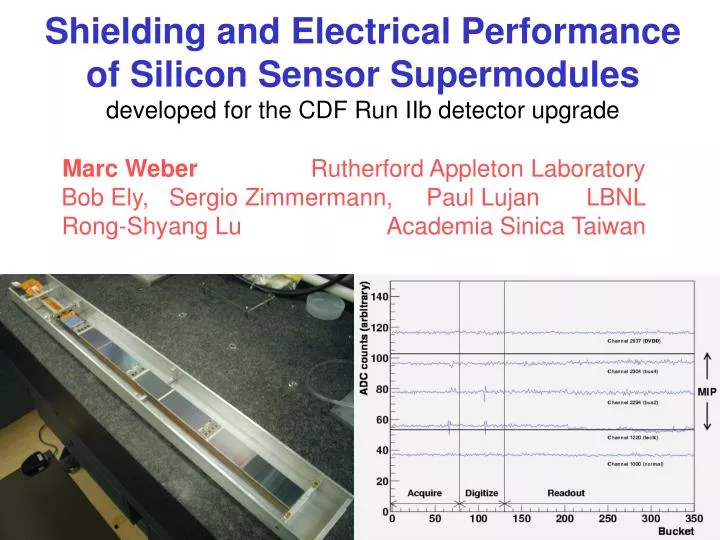
Shielding and Electrical Performance of Silicon Sensor Supermodules developed for the CDF Run IIb detector upgrade. Marc Weber Rutherford Appleton Laboratory Bob Ely, Sergio Zimmermann, Paul Lujan LBNL Rong-Shyang Lu Academia Sinica Taiwan.

E N D
Shielding and Electrical Performance of Silicon Sensor Supermodules developed for the CDF Run IIb detector upgrade Marc Weber Rutherford Appleton Laboratory Bob Ely, Sergio Zimmermann, Paul Lujan LBNL Rong-Shyang Lu Academia Sinica Taiwan
silicon sensors 4-chip hybrids back side front side What is a supermodule ? highly integrated mechanical, electrical and thermal structure; single-sided silicon strip sensors on top and bottom; 66 cm long; 3072 channels; low mass: 150 g; 1.7% of a radiation length
Supermodules or staves How to use a supermodule ? Barrel Bulkhead Services for CDF Run IIb: 2barrels with 192 supermodules around beampipe (+ Layer 0) • supermodules supported by bulkheads only => minimizes material • services at one end only => 1.2 m long 2-barrel construction Interesting design also for future hadron colliders
A closer look: schematic side view “simple”layerstructure: SVX4 chip on BeO hybrid onsingle-sided sensor on bus cable oncarbon fiber/foam core • hybrid is wire-bonded to bus cable through 3 mm gap between pairs of sensors • bus cable copper traces stop after reaching 3. hybrid • 25/50 μm thick aluminum shields under each sensor pair, connected to hybrid ground (AG=DG=HG) • top and bottom side nearly symmetric, but typically axial strips on top and 1.2stereo strips on bottom
Advantages • compact, light weight, radiation hard components • “easy” to build => fast construction, cheap, reliable • ideal for assembly: integrated services, modular detector • proximity ofsensors and bus cable can cause systematic pedestal shifts (“pick-up”)=> “fake hits”, noise occupancy, etc. • CDF runs in deadtime-less mode (data acquisition during “noisy” digitize and readout) to increase trigger bandwidth • requires understanding and suppression of conductive and capacitive interference mechanisms (see IEEE Trans. Sci., vol. 51, no. 3, pp. 987-993, June 2004) Challenges
Bus cable layout • single 18 μm thick copper layer (minimize material) • 25 μm or 50 μm thick aluminum shield between copper and silicon sensors • wide power traces; joint digital grounds; etc. to minimize IR drops Layout of a low-tech component crucial for system performance
plot shows pedestal of arbitrary channels as a function of time/ chip mode every channel with “signal” above average pedestal by “2-3” x noise will be read out and used in tracking algorithms • BE_CLK :______________________________ • COMP_RST:XXXXXXXXXXXXXXXX___________ • RREF_SEL:XXXXXXXXXXXXXXXXXXX________ • FE_MODE :87XXXXXXXXXXXXXXXXXXX90XXX • FE_CLK :T______T______T______T______T_ • L1A :XXXXXXXXXXXXXXXXXXXXXXXXXX • PRD1 :_____XXXXX________________XXXX • Excellent performance ! Electrical Performance Noise: ~2ADC counts/1000 e bits of a control pattern a bucket but one puzzle remained …
plot shows pedestal of all channels at arbitrary time (front-side, 25 μm shield,3 hybrids superimposed) every channel with “signal” above average pedestal by “2-3” x noise will be read out and used in tracking algorithms What is this structure ? ( 50 ADC = 1 MIP) Electrical Performance Pick-up above FE clock line !
plot shows pedestal of all channels at an arbitrary time no pick-up if: • 1.2stereo strips (at supermodule bottom side) • no clock lines under sensor (at 3. sensor pair) • 50 μm thick aluminum shield (final layout) Different experimental setups ( 50 ADC = 1 MIP) => CDF supermodule design OK, butWhat is the interference mechanism ?
(strips and clock traces run into slide plane, not to scale !) layer thicknesses: Sensor: 320 μm Adhesive: 25 μm Kapton: 25 μm Adhesive: 25 μm Aluminum: 25/50 μm Adhesive: 25 μm Copper: 18 μm Kapton: 25 μm … Transverse supermodule X-section p-implants, AC coupling, ~40 μm pitch, every 2. strip is read out Sensor 75 μm width/ 100 μm space CLOCK CLOCK_B Would like to understand width and size of pick-up
• front-end clock signal => time-dependent magnetic fields => Eddy currents in aluminum shield => current produces magnetic field seen by the silicon strips • adjacent strips form loop (through preamplifier ground and interstrip capacitance) => time-dependent magnetic flux perpendicular to loop leads to emf => net current into preamplifier: “pick-up” Interference mechanism X Axis Strip Interstrip capacitance Strip Strip Z axis - L/2 L/2
Analytical approach following Smythe: Eddy currents in infinite plane sheet by image method x is coordinateperpendicular to shield and strips; z is coordinatealong strips z Numerical approach using Maxwell 2D program from Ansoft: decent agreement of results Various approximations: only 10 Fourier harmonics to parameterize time-dependence of fields; consider only 19 adjacent strips; use only dominant pole to describe SVX4 preamp rise times; >10% uncertainty in clock driver currents; 2D model; ignored carbon fiber at supermodule core; etc. Calculation of B
Comparison with simulation • data averaged over 180 events, excellent data quality • here “extreme” scenario chosento maximize effect: thin aluminum shield ( 25 μm); max. driver current ( ~20 mA); min. rise time • width and size of simulation ~30% too small (in our approximations) , but Main effect reproduced by simulation Data Simulation
What influences size of interference ? • Clock driver currents: pick-up proportional to driver current; reduction by factor 2 for minimum current • Aluminum shield thickness(50 μm and 25 μm): Simulation: reduction by factor ~5 with 50 μm shield Data: no pick-up for thick shield(in standard clock pattern) • Preamp bandwidth/rise times: pick-up reduced with increasing preamp rise time in data and simulation (by > factor 2) • [ Clock frequencies: little variation in data when reducing clock frequency from 50 MHz by factor 4.5 ] Huge collection of data, so far always consistent with simulation
Given a quantitative model of typical interference effects: • less prototyping needed • can optimize system components ( transceivers, readout chips, bus cable) at early design stages • simple design choices can have big effect: e.g. small 1.2angle between strips and clock traces (rotate strips or rotate traces !)
Summary/Conclusions • local pedestal fluctuations in strips above a clock trace observed in prototype supermodules • Time-dependent magnetic fields, associated with clock signals, induce an emfin adjacent strips, which leads to a net charge flow into preamp • Numerical and analytical calculations of this effect agree with the data • the fields can be suppressed efficiently by a thin aluminum shield Quantitative estimate of interference effects possible, gives superior system design Electrical performance of CDF Run IIb supermodules is excellent Compact packaging can be combined with deadtime-less operation
plot shows pedestal of arbitrary channel as a function of time/ chip mode every channel with “signal” above average pedestal by “2-3” x noise will be read out and used in tracking algorithms • BE_CLK :______________________________ • COMP_RST:XXXXXXXXXXXXXXXX___________ • RREF_SEL:XXXXXXXXXXXXXXXXXXX________ • FE_MODE :87XXXXXXXXXXXXXXXXXXX90XXX • FE_CLK :T______T______T______T______T_ • L1A :XXXXXXXXXXXXXXXXXXXXXXXXXX • PRD1 :_____XXXXX________________XXXX Fair performance (if RTPS) , but final design is much better ! Electrical Performance: prototype bits of a control pattern a bucket
X Axis Strip Strip Strip Z axis - L/2 L/2 Interstrip capacitance