Download
1 / 45
510 likes | 921 Views
Optics on Graphene. Gate-Variable Optical Transitions in Graphene Feng Wang , Yuanbo Zhang, Chuanshan Tian, Caglar Girit, Alex Zettl, Michael Crommie, and Y. Ron Shen, Science 320, 206 (2008). Direct Observation of a Widely Tunable Bandgap in Bilayer Graphene

E N D
Gate-Variable Optical Transitions in Graphene Feng Wang, Yuanbo Zhang, Chuanshan Tian, Caglar Girit, Alex Zettl, Michael Crommie, and Y. Ron Shen,Science 320, 206 (2008). Direct Observation of a Widely Tunable Bandgap in Bilayer Graphene Yuanbo Zhang, Tsung-Ta Tang, Caglar Girit1, Zhao Hao, Michael C. Martin, Alex Zettl1, Michael F. Crommie, Y. Ron Shen and Feng Wang(2009)
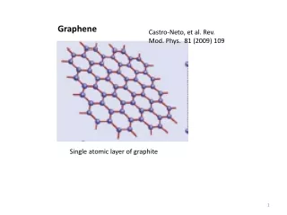
Graphene(A Monolayer of Graphite) 2D Hexagonal lattice
Properties of Graphene Electrically: High mobility at room temperature, Large current carrying capability Mechanically: Large Young’s modulus. Thermally: High thermal conductance.
Exotic Behaviors Quantum Hall effect, Barry Phase Ballistic transport, Klein paradox Others
Quantum Hall Effect Y. Zhang et al, Nature438, 201(2005)
Other Possibilites • Spectroscopic probe of electronic structure. • Interlayer coupling effect. • Electrical gating effect on optical transitions. • Others Optical Studies of Graphene Optical microscopy contrast; Raman spectroscopy; Landau level spectroscopy.
Graphene 2D Hexagonal lattice
Band Structure of Graphene Monolayer P.R.Wallace, Phys.Rev.71,622-634(1947)
Band Structure near K Points Relativistic Dirac fermion. ~10 eV
Band Structures of Graphene Monolayer and Bilayer near K Bilayer Monolayer x K K x Vertical optical transition Van Hove Singularity EF is adjustable
Exfoliated Graphene Monolayers and Bilayers Reflecting microscope images. 20 m Monolayer Bilayer K. S. Novoselov et al., Science306, 666 (2004).
Raman Spectroscopy of Graphene (Allowing ID of monolayer and bilayer) A.S.Ferrari, et al, PRL 97, 187401 (2006)
Experimental Arrangement Det OPA Gold Graphene 290-nm Silica Doped Si
Infrared Reflection Spectroscopyto Deduce Absorption Spectrum Differential reflection spectroscopy: Difference between bare substrate and graphene on substrate RA: bare substrate reflectivity RB: substrate + graphene reflectivity A 20 m B -dR/R (RA-RB)/RA versus w dR/R = -Re[h(w)s(w)] h(w) from substrate s(w) from graphene: interband transitons free carrier absorption Re s(w)/w: Absorption spectrum
Monolayer Spectrum dR/R 2EF x C: capacitance
Experimental Arrangement Det OPA Gold Graphene 290-nm Silica Vg Doped Si
dR/R 2EF Gate Effect on Monolayer Graphene X X X Small density of states close to Dirac point E = 0 Carrier injection by applying gate voltage can lead to large Fermi energy shift . EF can be shifted by ~0.5 eV with Vg ~ 50 v; Shifting threshold of transitions by ~1 eV If Vg = Vg0 + Vmod, then should be a maximum at
Vary Optical Transitions by Gating Vary gate voltage Vg. Laser beam Measure modulated reflectivity due to Vmod at V ( Analogous to dI/dV measurement in transport)
= 350 meV Results in Graphene Monolayer The maximum determines Vg for the given EF.
Mapping Band Structure near K dR/R 2EF For different w, the gate voltage Vgdetermined from maximum is different, following the relation , Slope of the line allows deduction of slope of the band structure (Dirac cone)
2D Plot of Monolayer Spectrum Experiment Theory
Strength of Gate Modulation Vg = 0 D(dR/R) (dR/R)60V-(dR/R) -50V
Band Structure of Graphene Bilayer For symmetric layers, D = 0 For asymmetric layer, D 0 E. McCann, V.I.Fal’ko, PRL 96, 086805 (2006);
Doubly Gated Bilayer Asymmetry: D D (Db + Dt)/2 0 Carrier injection to shift EF: F dD = (Db - Dt)
Sample Preparation Effective initial bias due to impurity doping
Transport Measurement Maximum resistance appears at EF = 0 Lowest peak resistance corresponds to Db = Dt = 0 .
Optical Transitions in Bilayer I: Direct gap transition (tunable, <250 meV) II, IV: Transition between conduction/valence bands (~400 meV, dominated by van Hove singularity) III, V: Transition between conduction and valence bands (~400 meV, relatively weak) If dEF=0, then II and IV do not contribute
Bandstructure Change Induced by x IV II x Transitions II & IV inactive Transition I active
Differential Bilayer Spectra (dD = 0)(Difference between spectra of D0 and D=0) I I IV Larger bandgap stronger transition I because ot higher density of states
Charge Injection without Change of Bandstructure (D fixed) dD 0 dD = 0 x IV III Transition IV becomes active Peak shifts to lower energy as D increases.. Transition III becomes weaker and shifts to higher energy as D increases.
Difference Spectra for Different D betweendD=0.15 v/nm and dD=0
Strength of Gate Modulation D(dR/R) (dR/R)60V-(dR/R) -50V is comparable to dR/R in value
Summary • Grahpene exhibits interesting optical behaviors:. • Gate bias can significantly modify optical transitions over a broad spectral range. • Single gate bias shifts the Fermi level of monolayer graphene. • Spectra provides information on bandstructure, allowing deduction of VF(slope of the Dirac cone in the bandstructure). • Double gate bias tunes the bandgap and shifts the Fermi level of bilayer • graphene. • Widely gate-tunable bandgap of bilayer graphene could be useful in future device applications. • Strong gating effects on optical properties of graphene could be useful in infrared optoelectronic devices.