Download
1 / 9
130 likes | 475 Views
Epitaxial graphene. Claire Berger GATECH- School of Physics, Atlanta CNRS-Institut Néel, Grenoble. NIRT Nanopatterned Epitaxial graphite. Motivation :. Carbon nanotube transistors. Motivation :. Multiwalled carbon nanotubes are ballistic conductors at room temperature. - L (µm).

E N D
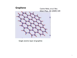
Epitaxialgraphene Claire Berger GATECH- School of Physics, Atlanta CNRS-Institut Néel, Grenoble NIRT Nanopatterned Epitaxial graphite
Motivation : Carbon nanotube transistors
Motivation : Multiwalled carbon nanotubes are ballistic conductors at room temperature - L (µm) T. Ando, T. Nakanishi and R. Saito J. Phys. Soc. Jpn. 67, 2857 (1998) “The absence of backward scattering is shown to be ascribed to Berry's phase which corresponds to a sign change of the wave function under a rotation of a neutrino-like particle*in the wave vector space in a two-dimensional graphite” *i.e obeying the Dirac-Weyl equation G (2e2/h) Nanotube fiber L V Quantized ballistic conductance
Nanotube Electronic Structure EF 1D metallic sub-bands Semiconducting Ntube
Band structure of graphene Linear dispersion Symmetry electrons - holes Pseudospin Chirality T. Ando, J. Phys. Soc. Jpn 67 (1998) 2857
Graphene ribbons Semiconducting or metallic ribbons Metallic ribbons Graphene ribbons should retain the essential properties of carbon nanotubes
Energy gap in exfoliated graphene ribbons from Philip Kim, Columbia University E=0.2 eV.nm W*=16 nm Gap Eg=E /(W-W*) M. Y. Han, B. Özyilmaz, Y. Zhang, P. Kim, Cond. Mat. 0702511
Epitaxial growth of graphene layers on 4H-SiC Si Si Si C (0001) Si-face SiC (0001) C-face graphite SiC Graphene on SiC Thermal decomposition of SiC at high temperature (~1400oC) - high vacuum after surface flattening by hydrogen etching A.Charrier et al., J. Applied Physics 92, 2479 (2002) LEED 3 graphene layers By controling temperature, growth of 1 to ~100 graphene layers C. Berger et al., Journal of Physical Chemistry B 108, 19912 (2004)