Download
1 / 45
480 likes | 610 Views
Explore the crystal structure of semiconductors through defects, CZ and FZ growth, bonding types, and lattice properties. Learn about atomic bonding, impurities, and the different classes of solid-state materials.

E N D
DMT 234 SEMICONDUCTOR PHYSICS & DEVICE Lecture 2The Crystal Structure of Solids Nor Roshidah 2012
SUBTOPIC Point defect Line defect CZ FZ Crystal Growth Si, Ge Elementary Frenkel defect Imperfection Impurities S/c material GaAs, GaN InGaN, AlGaAs Compound CRYSTAL STRUCTURE OF SOLIDS Crystal Structure Types amorphous Bonding ionic polycrystalline covalent Single crystalline metallic Van de Walls Structure Direction Crystal plane simple BCC FCC
SOLID STATE MATERIAL Solid state material can be grouped into 3 classes
DIFFERENT TYPES OF SOLIDS • i. Amorphous • little or no order • ii. Polycrystalline • High degree of order within limited regions which vary in size and orientation to each other. • iii. Single Crystal • High degree of order throughout the entire volume • of the material.
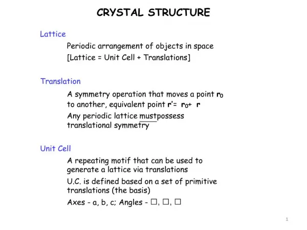
CRYSTAL STRUCTURE SPACE LATTICES • The regular geometric periodicity in the atomic arrangement. • Lattice –periodic arrangement of atoms in crystal. • Lattice point – a particular atomic array shown by a dot. These dots are separated (translated) in certain directions and dimensions • Unit Cell – a small volume of the crystal that can be used to reproduce the entire crystal.
CRYSTAL STRUCTURE PRIMITIVE CELL AND LATTICE VECTOR • Primitive cell – the smallest unit cell that can be repeated to form the lattice. • Lattice vector – every equivalent lattice point in the three-dimensional crystal can be found by using the vector : • Where p, q and s are integers.
CRYSTAL STRUCTURE BASIC CRYSTAL STRUCTURES
CRYSTAL STRUCTURE SIMPLE CUBIC Number of atom per unit cell (A) : 1/8 x 8 = 1 Volume of unit cell (B) : a3 Volume density of atom = A/B = 1/ a3
CRYSTAL STRUCTURE FACE-CENTERED CUBIC Number of atom per unit cell (A) : (1/8 x 8) + (1/2 x 6) = 4 Volume of unit cell (B) : a3 Volume density of atom = A/B = 4/ a3
CRYSTAL STRUCTURE BODY-CENTERED CUBIC Number of atom per unit cell (A) : (1/8 x 8) + 1 = 2 Volume of unit cell (B) : a3 Volume density of atom = A/B = 2/ a3
exercise Find the volume density of atoms in crystal for :- • Figure a, if lattice constant, a = 5 x 10⁻⁸cm • Figure b, if lattice constant, a = 4.25 x 10⁻⁸ cm Figure a Figure b
CRYSTAL STRUCTURE how to identify types of the wafer?? Is it p-type or n-type wafer?? Is it (100), (111) or (101) orientation??
CRYSTAL STRUCTURE Different plane orientation shows a different shape of wafer
CRYSTAL PLANE Describe the plane shown in this figure ??
CRYSTAL PLANE EXERCISE Figure 1 Figure 2 Describe the plane of the above figure ??
DIRECTION IN CRYSTAL Plane (hkl) ; Direction [hkl] Note : for the simple cubic lattice , (hkl) is perpendicular to [hkl]
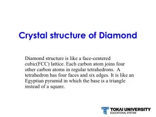
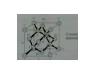
DIAMOND STRUCTURE(SILICON, germanium) 1/2 0 0 3/4 1/4 1/2 1/2 0 1/4 3/4 • this structure belongs to FCC crystal family • 2 FCC sublattice with one sublattice displaces from the other by one-quarter of the distance • Total number of atom = 8 • 8 corner atoms x 1/8 = 1atom • 6 face atoms x 1/2 = 3 atoms • 4 enclosed atoms = 4 atoms 0 1/2 0
DIAMOND STRUCTURE • Tetrahedral bonding structure • BCC structure with 4 nearest neighbors • This is the basic building block of diamond lattice
ZINCBLENDE STRUCTURE(GALLIUM ARSENIDE) • Zincblende structure is same as diamond structure except it have 2 different types of atom in lattice i.e : Ga and As
IMPERFECTIONS IN SOLIDS • Lattice imperfection : any deviation from perfect periodic arrangement of lattice points. • Effect : Change electrical and optical properties
IMPERFECTIONS IN SOLIDS Vacancy Interstitial Volume Plane Line dislocation
IMPURITIES IN SOLIDS • Impurities:occurs due to the present of foreign/ impurities atoms especially during doping process (ion implantation / diffusion) • Types :- • Substitutional impurity • Interstitial impurity
GROWTH OF SEMICONDUCTOR CRUCIBLE NO CRUCIBLE
DMT 234 Semiconductor Physic & Device Growth of Semiconductor Materials
DMT 234 Semiconductor Physic & Device Growth of Semiconductor Materials
DMT 234 Semiconductor Physic & Device Growth of Semiconductor Materials
DMT 234 Semiconductor Physic & Device Growth of Semiconductor Materials
DMT 234 Semiconductor Physic & Device Growth of Semiconductor Materials
DMT 234 Semiconductor Physic & Device Growth of Semiconductor Materials
DMT 234 Semiconductor Physic & Device Growth of Semiconductor Materials
DMT 234 Semiconductor Physic & Device Growth of Semiconductor Materials
DMT 234 Semiconductor Physic & Device Growth of Semiconductor Materials
DMT 234 Semiconductor Physic & Device Growth of Semiconductor Materials
DMT 234 Semiconductor Physic & Device • Q & A • Next week Topic :The Semiconductor in Equilibrium.