Download
1 / 25
250 likes | 338 Views
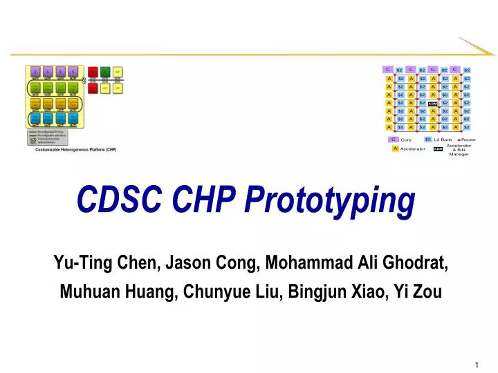
CDSC CHP Prototyping. Yu-Ting Chen, Jason Cong, Mohammad Ali Ghodrat, Muhuan Huang, Chunyue Liu, Bingjun Xiao, Yi Zou. Accelerator-Rich Architectures: ARC, CHARM, BiN. Goals. Implement the architecture features & supports into the prototype system Architecture Proposals

E N D
CDSC CHP Prototyping Yu-Ting Chen, Jason Cong, Mohammad Ali Ghodrat, Muhuan Huang, Chunyue Liu, Bingjun Xiao, Yi Zou
Goals • Implement the architecture features & supports into the prototype system • Architecture Proposals • Architecture-rich CMPs • CHARM • Hybrid cache • Buffer-in NUCA etc • Bridge different thrusts in CDSC
Server-Class Platform: HC-1ex Architecture • XC6vlx760 FPGAs • 80GB/s off-chip bandwidth • 90W Design Power Xeon Quad Core LV5408 40W TDP Tesla C1060 100GB/s off-chip bandwidth 200W TDP
Drawback of the Commodity Systems • Limited ability to customize from the architecture point of view • Board-level integration rather than chip-level integration • Commodity systems can only reach certain-level, we need further innovations
CHP Prototyping Plan • Create the working hardware and software • Use FPGA Extensible Processing Platform (EPP) as the platform • Reuse existing FPGA IPs as much as possible • Working in multiple phases
Target Platforms: Xilinx ML605 and Zynq • Dual-core A9 with programmable logics • Virtex6-based board
CHP Prototyping Phases • ARC Implementation • Phase 1: Basic platform • Accelerator and Software GAM • Phase 2: Adding modularity using available IP • E.g. Xilinx DMAC IP • Phase 3: First step toward BiN • Shared buffer • Customized modules (e.g. DMA-controller, plug-n-play accelerator) • Phase 4: System Enhancement • Crossbar • AXI implementation • CHARM Implementation
ARC Phase 1 Goals • Setting up a basic environment • Multi-core + simple accelerators + OS • Understanding the system interactions in more detail • Simple controller as GAM (global accelerator manager) • Supports sharing at system-level for multiple accelerators of a same type
ARC Phase 1 Example System Diagram Microblaze-0 (Linux with MMU) Mailbox (vecadd) Microblaze-1 (GAM) (Bare-metal; no MMU) FSL Mailbox (vecsub) FSL FSL AXI4 (xbar) FSL AXI4lite (bus) timer mutex uart DDR3 vecadd vecsub vecadd vecsub
ARC Phase-2 Goals • Implementing a system similar to ARC original design • GAM, Accelerator, DMA-Controller, SPM • Adding modularity using available IP • E.g. Xilinx DMAC IP
ARC Phase-2 Performance and Power Results • Benchmarking kernel: • Results
ARC Phase-2 Area Breakdown • Slice Logic Utilization • Number of Slice Registers: 45,283 out of 301,440: 15% • Number of Slice LUTs: 40,749 out of 150,720: 27% • Number used as logic: 32,505 out of 150,720: 21% • Number used as Memory: 5,248 out of 58,400: 8% • Slice Logic Distribution: • Number of occupied Slices: 17,621 out of 37,680: 46% • Number of LUT Flip Flop pairs used: 54,323 • Number with an unused Flip Flop: 14,617 out of 54,323: 26% • Number with an unused LUT: 13,574 out of 54,323: 24% • Number of fully used LUT-FF pairs: 26,132 out of 54,323: 48%
ARC Phase-3 Goals • First step toward BiN: • Shared buffer • Designing our customized modules • Customized DMA-controller • Handles batch TLB misses • Plug-n-play accelerator design • Making the interface general enough at least for a class of accelerators
ARC Phase-3 Architecture • A partial realization of the proposed accelerator-rich CMP onto Xilinx ML605 (Virtex-6) • Global accelerator manager (GAM) for accelerator sharing • Shared on-chip buffers: Much more accelerators than buffer bank resources • Virtual addressing in the accelerators, accelerator virtualization • Virtual addressing DMA, with on-demand TLB filling from core • No network-on-chip, no buffer sharing with cache, no customized instruction in the core
Performance and Power Results • Benchmarking kernel: • Results
Impact of Communication & Computation Overlapping Pipelined Communication & Computation 19% No pipeline
Overhead of Buffer Sharing: Bank Access Contention (1) The 4 logic buffers are allocated to 4 separate buffer banks Reason: AXI bus allow masters simultaneously issue transactions. and the AXI transaction time dominates buffer access time 3.2% The 4 logic buffers are allocated to 1 buffer bank
Overhead of Buffer Sharing: Bank Access Contention (2) The 4 logic buffers are allocated to 4 separate buffer banks 2.7% The 4 logic buffers are allocated to 1 buffer bank
Area Breakdown • Slice Logic Utilization • Number of Slice Registers: 105,969 out of 301,440: 35% • Number of Slice LUTs: 93,755 out of 150,720: 62% • Number used as logic: 80,410 out of 150,720: 53% • Number used as Memory: 7,406 out of 58,400: 12% • Slice Logic Distribution: • Number of occupied Slices: 32,779 out of 37,680: 86% • Number of LUT Flip Flop pairs used: 112,772 • Number with an unused Flip Flop: 25,037 out of 112,772: 22% • Number with an unused LUT: 19,017 out of 112,772: 16% • Number of fully used LUT-FF pairs: 68,718 out of 112,772: 60%
Phase-4 ARC Goals • Finding bottlenecks and system enhancement • Communication bottleneck • Crossbar design instead of AXI-bus • Speed-up AXI non-burst implementation
Accelerator Memory System Design • Crossbar • In addition to previously proposed • now support partial configuration • will not affect working LCAs • Passed on-board test • Hierarchical DMACs • Data transfer between • Main memory • Shared buffer banks • # of buffer banks can be large • want to keep AXI bus size • Hierarchical DMACs and buses OC core IOMMU AXI buses Buffer bank1 LCA1 DMAC1 Buffer bank2 LCA2 Main AXI bus Buffer bank3 DMAC2 LCA3 Buffer bank4 LCA4 DMAC3 Buffer bank9 Select-bit Receiver to DDR GAM