Download
1 / 12
120 likes | 258 Views
ECAL Si sensors status and plans May 2006. V.Vrba. Status. EUDET prototype : end of 2005: production of 20 wafers produced at ON Semiconductor, tested at Prague good quality; beginning of 2006: wafers delivered to Ecole Polytechnique – no report about any problem;. :

E N D
ECAL Si sensors status and plansMay 2006 V.Vrba Václav Vrba, Institute of Physics, AS CR
Status • EUDET prototype: • end of 2005: production of 20 wafers produced at ON Semiconductor, tested at Prague good quality; • beginning of 2006: wafers delivered to Ecole Polytechnique – no report about any problem; • : • April 2006: ordered next batch of about 60 wafers at On Semiconductor to be ready ~ June 5, then measured and delivered to Ecole Polytechnique ~ June 15 • waiting for news from news from Ecole Polytechnique; • looking forward for new delivery from ON Semiconductor. Václav Vrba, Institute of Physics, AS CR
Recent developments • 4x4 pad sensor array produced @ONSemiconductor with poly-silicon resistors • Layout of components on the wafer: Václav Vrba, Institute of Physics, AS CR
I-V and C-V on single diodes Václav Vrba, Institute of Physics, AS CR
I-V curves for 4x4 pad array Václav Vrba, Institute of Physics, AS CR
Reverse current long term stability Václav Vrba, Institute of Physics, AS CR
Polysilicon resistors • : • Polysilicon resistors ~ 1.2MOhm +/- ~30% • can be improved by optimization of resistor shape (minimize fluctuationd due to etching), better tuning of lithography etc. Václav Vrba, Institute of Physics, AS CR
Plans (1) • New design: • smaller size: from 10 mm pitch to ~ 5 mm pitch; • different shapes: hexagonal shape gives better two-dimensional resolution then square shape (by approx 30%) – or – the same resolution with less number of electronic channels; Václav Vrba, Institute of Physics, AS CR
Plans (2) • Precision layer (s ?): • better determination of the shower position, shower disentangling etc; • pre-shower layer? • needs simulation for optimal position and cell size for the given detector spatial configuration. Václav Vrba, Institute of Physics, AS CR
Investigation of possibility of use of 6“ wafers Václav Vrba, Institute of Physics, AS CR
Summary • : • production of wafers for EUDET module in progress shall be in time; • proved possibility of fabrication of integrated bias resistors no visible reduction of production yield; • studies of fine granularity, different pad shape, precision layer, pre-shower layer are in progress; • possibility of the use of 6” wafers is also investigated. Václav Vrba, Institute of Physics, AS CR
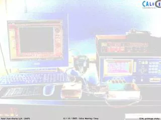
Sensor probing @ Institute of Physics • V r. 2006: testování cca 30-40% dodatečné produkce senzorů. Pracoviště pro měření pixelových detektorů ve Fyzikálním ústavu Senzory vyrobené v ON Semiconductor CR (dříve TESLA Sezam) Václav Vrba, Institute of Physics, AS CR