Download
1 / 9
90 likes | 231 Views
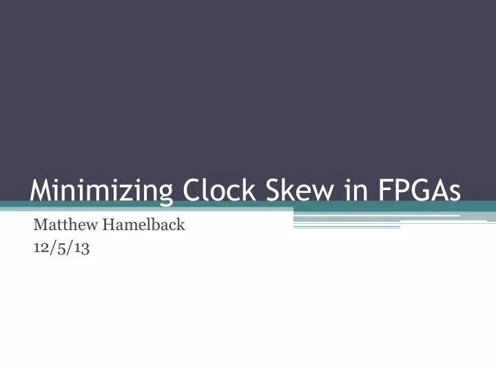
Minimizing Clock Skew in FPGAs. Matthew Hamelback 12/5/13. FPGA. Field Programmable Gate Array IC designed to by configured by customer Uses logic gates and RAM blocks to implement digital computations Fast I/Os and bidirectional data buses Challenge to get correct timing.

E N D
Minimizing Clock Skew in FPGAs Matthew Hamelback 12/5/13
FPGA • Field Programmable Gate Array • IC designed to by configured by customer • Uses logic gates and RAM blocks to implement digital computations • Fast I/Os and bidirectional data buses • Challenge to get correct timing
Solutions to Minimize Clock Skew • Placement • Clock Tree Architecture (H-Tree versus Comb) • Selection of modules / logic blocks • Registers • Pipelining • Wave pipelining • Direction of new algorithms
Clock Tree Architecture Comb H-Tree • Clock signal passed down the spine then spreads out through the branches • Does not have equal length traces • All trace lengths are equal • Minimizes clock skew clock
Selection of Modules Clock skew unaffected Clock skew affected • Each module or logic block has a resistance and load capacitance • Spreading out modules balances the load capacitance and the clock skew is not majorly affected • Equivalent RC circuit of trace with the clockpin connected or disconnected: Not connected Connected
Pipelining • Increases operating frequency by dividing the combinational logic into stages • Registers are used in between stages • Takes advantage of parallel processing • Max clock rate is limited to the longest path of a single stage versus all stages together
Wave Pipelining • Maximum rate pipelining • Logic propagation depends on difference between longest and shortest traces • Shaded region – Unstable • Unshaded region - Stable • Goal is equalization of path delays and minimizes unstable periods • Improves speed with less area and clock load • Uses an enable (en) signal to opening of output latch only when in the stable region
New Direction of Algorithms for FPGAs • Traditional placement algorithms: • Minimize area • Minimize total wire lengths • Satisfy timing requirements • New placement algorithms for FPGAs have primary objective of minimizing clock skew depending on selected logic modules
References 1. Clock Skew Minimization During FPGA Placement (Zhu, Wong) http://ieeexplore.ieee.org.www2.lib.ku.edu:2048/stamp/stamp.jsp?tp=&arnumber=602474 2. A Novel Online Clock Skew Scheme (Santhi) http://ieeexplore.ieee.org.www2.lib.ku.edu:2048/stamp/stamp.jsp?tp=&arnumber=5482689 3. Exploiting Clock Skew Scheduling for FPGA (Bae) http://ieeexplore.ieee.org.www2.lib.ku.edu:2048/stamp/stamp.jsp?tp=&arnumber=5090904 4. DLL-Based Multi-FPGA systems clock (Cheng-chang) http://ieeexplore.ieee.org.www2.lib.ku.edu:2048/stamp/stamp.jsp?tp=&arnumber=5514852