Download
1 / 1
10 likes | 191 Views
Lightweight electronics and displays IRG4 MRSEC Tobin J. Marks, Mark A. Ratner, Pulak Dutta Northwestern University DMR-0076097.

E N D
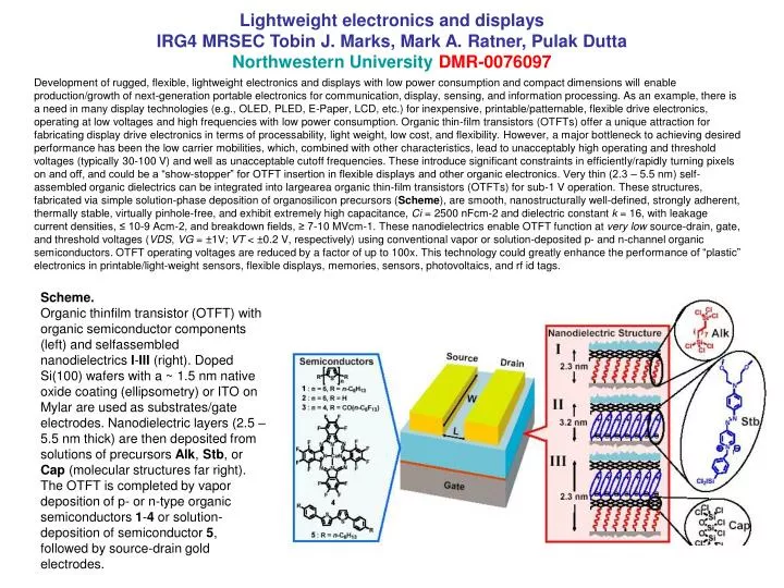
Lightweight electronics and displaysIRG4 MRSEC Tobin J. Marks, Mark A. Ratner, Pulak DuttaNorthwestern University DMR-0076097 Development of rugged, flexible, lightweight electronics and displays with low power consumption and compact dimensions will enable production/growth of next-generation portable electronics for communication, display, sensing, and information processing. As an example, there is a need in many display technologies (e.g., OLED, PLED, E-Paper, LCD, etc.) for inexpensive, printable/patternable, flexible drive electronics, operating at low voltages and high frequencies with low power consumption. Organic thin-film transistors (OTFTs) offer a unique attraction for fabricating display drive electronics in terms of processability, light weight, low cost, and flexibility. However, a major bottleneck to achieving desired performance has been the low carrier mobilities, which, combined with other characteristics, lead to unacceptably high operating and threshold voltages (typically 30-100 V) and well as unacceptable cutoff frequencies. These introduce significant constraints in efficiently/rapidly turning pixels on and off, and could be a “show-stopper” for OTFT insertion in flexible displays and other organic electronics. Very thin (2.3 – 5.5 nm) self-assembled organic dielectrics can be integrated into largearea organic thin-film transistors (OTFTs) for sub-1 V operation. These structures, fabricated via simple solution-phase deposition of organosilicon precursors (Scheme), are smooth, nanostructurally well-defined, strongly adherent, thermally stable, virtually pinhole-free, and exhibit extremely high capacitance, Ci = 2500 nFcm-2 and dielectric constant k = 16, with leakage current densities, ≤ 10-9 Acm-2, and breakdown fields, ≥ 7-10 MVcm-1. These nanodielectrics enable OTFT function at very low source-drain, gate, and threshold voltages (VDS, VG = ±1V; VT < ±0.2 V, respectively) using conventional vapor or solution-deposited p- and n-channel organic semiconductors. OTFT operating voltages are reduced by a factor of up to 100x. This technology could greatly enhance the performance of “plastic” electronics in printable/light-weight sensors, flexible displays, memories, sensors, photovoltaics, and rf id tags. Scheme. Organic thinfilm transistor (OTFT) with organic semiconductor components (left) and selfassembled nanodielectrics I-III (right). Doped Si(100) wafers with a ~ 1.5 nm native oxide coating (ellipsometry) or ITO on Mylar are used as substrates/gate electrodes. Nanodielectric layers (2.5 – 5.5 nm thick) are then deposited from solutions of precursors Alk, Stb, or Cap (molecular structures far right). The OTFT is completed by vapor deposition of p- or n-type organic semiconductors 1-4 or solution-deposition of semiconductor 5, followed by source-drain gold electrodes.